
MOST OF THE CONSTRUCTION work involves building the two PCB assemblies used in the counter. Before building these boards, however, note that we’ve made a few changes to the circuit published last month in order to achieve optimum performance. This involves a few component value changes, plus the addition of two extra components.
The details of these changes are given in the panel titled ‘Circuit Changes’ (towards the end of this article). This panel should be read carefully before beginning construction.
As mentioned in Part 1, most of the parts are fitted on a 225 x 175mm main PCB which mounts in the lower half of the case. The rest of the components are for the multiplexed display and these go on a second 200 x 50mm display PCB mounted vertically behind the front panel. The two boards are linked by a short 20-way ribbon cable fitted with IDC connectors.
Display PCB
Start the assembly by building the display PCB - see Fig.6. This carries the 7-segment displays, the LEDs, IC25 and IC26 and all the resistors and capacitors on the front. The other side carries 23 SMD MOSFETs (Q8-Q30) plus connector CON6, which is the header for the IDC cable.
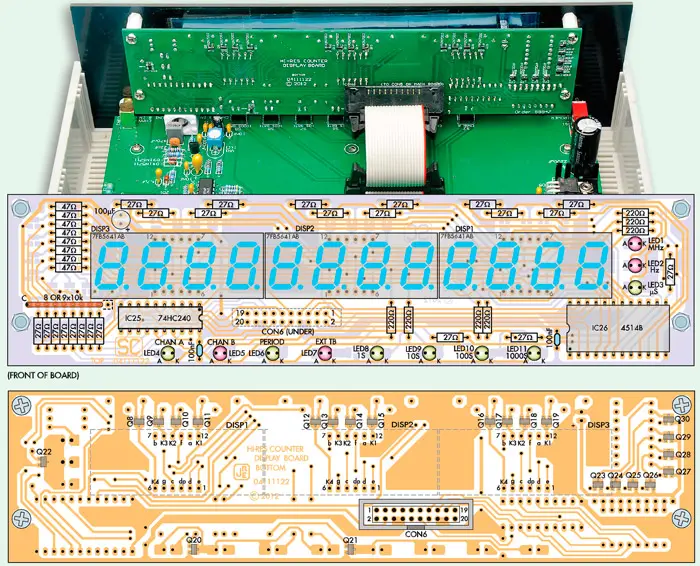
Fig.6: follow these parts layout diagrams to build the display PCB, starting with the SMD transistors (Q8-Q30) and IDC connector CON6 on the back of the board. Take care with the orientation of the LED readouts and note that IC25 and IC26 face in opposite directions.
The 23 SMD MOSFETs on the rear of the PCB should be installed first. Note that you must use 2N7002 N-channel devices for Q8-Q22 and NX2301P P-channel MOSFETs for Q23-Q30. Don’t mix them up, or you’ll get some very strange results!
You’ll need a soldering iron with a fine tip, a pair of tweezers and preferably a magnifying lamp for this job. Start by applying some solder to one of the PCB pads and then, using the tweezers, slide the device into place while heating the solder on the pad. That done, check that the part is correctly positioned. If not, reheat the solder and gently nudge it into place.
The remaining two leads can then be soldered. If you get a solder bridge, simply use desoldering braid (or solder wick) to clean it up. A dab of no-clean flux paste on the bridge beforehand will make it disappear a lot more quickly and easily.
Repeat this procedure for all 23 SMD MOSFETs, taking care to fit the correct type at each location. Once these are in place, fit CON6 then turn the PCB over and solder its pins to the pads on the front. Make sure that CON6 sits flush against the PCB before soldering.
The next step is to install the resistors on the front of the PCB, followed by the 8 x 10kQ SIL resistor array. Be sure to fit the latter with its common (C) pin towards the lefthand edge of the PCB. The two 100nF MMC capacitors and the 100pF electrolytic can then go in, followed by the three 4-digit LED displays, LEDs 1-11 and ICs 25 and 26. Take care with the orientation of these devices (note: the displays must be oriented with the decimal points at lower right).
The LEDs must be mounted with their bodies 10mm above the PCB, so that they will later protrude through their corresponding holes in the front panel. This can be done by sliding a 10mm-high strip of cardboard between the leads when soldering each device into position.
When all of these components are in place, the display PCB can be placed aside while you work on the main PCB.
Main PCB assembly
Like the display PCB, the main PCB has all of the SMD components mounted on one side (ie, the underside) and all of the leaded components on the top side. Figs.7 and 8 show the assembly details.
As before, it’s best to install the SMD parts on the underside first. Most of these SMDs are located inside the red rectangle at lower left. The only exceptions are transistors Q6 and Q7, which are located inside the red circle nearer the centre of the board - see Fig.7.
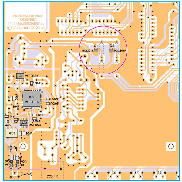
Fig.7: follow this layout diagram to mount the SMD parts on the rear of the main PCB (ie, the parts inside the red box and the red circle). Take care to ensure that the transistors, ICs and RFC3 are correctly oriented and note the bevelled end on one of IC1’s leads, indicating pin 1.
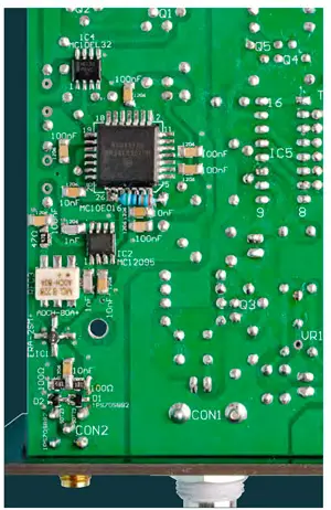
The view shows the SMD parts inside the red box of Fig.7. Ignore the resistor just below IC3; this is a modification to our prototype and the final PCB now has this on the top side.
Take particular care when installing IC1, IC2, IC3 and IC4 to ensure that they are correctly oriented. In each case, pin 1 is identified by an adjacent ‘dot’ in the plastic body of the device. IC3 also has a bevelled corner, while IC1 has a bevelled end on one lead.
Once again, you’ll need a soldering iron with a very fine tip, preferably one that is earthed to avoid electrostatic damage when you are soldering in the active components (IC1-IC4, Q6 and Q7 and D1 and D2). The iron should also be temperature controlled, so you can make joints quickly without risking heat damage to the component.
Table 1: Capacitor Codes
Value | μF Value | IEC Code | EIA Code |
470nF | 0.47μF | 470n | 474 |
100nF | 0.1 μF | 100n | 104 |
10nF | 0.01 μF | 10n | 103 |
1nF | 0.001 μF | 1n | 102 |
47pF | NA | 47p | 47 |
39pF | NA | 39p | 39 |
27pF | NA | 27p | 27 |
The soldering procedure is much the same as for the SMD MOSFETs on the display PCB. In each case, you can hold the device in place using tweezers (or even a wooden toothpick) while you make the first solder joint, after which the SMD should stay in position while you solder the remaining leads. However, if the device has eight or more leads, then it’s best to solder two diagonally opposite leads initially. The device can then be checked for correct alignment before the remaining leads are soldered.
Don’t worry too much if you accidentally bridge two or more of the leads of IC2, IC3 or IC4 together when you’re soldering them in place. In fact, this is almost inevitable. As before, it’s simply a matter of using the tip of the iron to push some fine desoldering braid against the bridged leads. The braid will ‘suck up’ the excess solder forming the bridge, while still leaving the leads soldered to the PCB pads underneath.
By the way, don’t forget to install RFC3, which is also an SMD component. It’s fitted in the same way as the SMD ICs and must also be correctly oriented (ie, pin 1 at top right).
When you have soldered all of the SMDs in place (including Q6 and Q7), the PCB can be flipped over and the leaded components installed. Fig.8 shows the details.
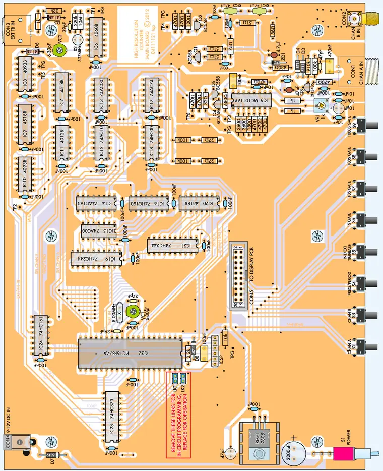
Fig.8: the parts on the top side of the main PCB should be installed only after the SMD parts have been installed on the underside. Be sure to fit the correct IC at each location and make sure that all polarised parts are correctly oriented.
Begin by installing the low-profile parts first, such as the resistors, diodes and Zener diodes. The 10 PC stakes can then be installed at the test points (TP). TP2 is required for calibration, while the remaining test points will make it much easier to troubleshoot the unit later on if necessary.
Trimpot VR1 can now go in (bottom right), followed by RF chokes RFC1 and RFC2 and then the non-polarised capacitors (including trimcaps VC1 and VC2). Follow with the polarised electrolytic and tantalum capacitors, taking care to fit them with the correct polarity.
Next, install connectors CON1-CON4, then pushbutton switches S2-S9, power switch S1, the 6-pin ICSP header and the two 2-pin headers for LK1 and LK2. CON5, the 20-pin DIL connector, can then be fitted.
Crystals X1 and X2 are next. X1 is located just to the right of IC22 (the PIC micro), while X2 is located just below VC2 at upper right. They can be fitted either way around.
Once, they’re in, install transistors Q1-Q5 and regulator REG1 (7805). The latter is mounted horizontally on the top of the PCB, with a 19mm-square finned heatsink underneath to help dissipate heat. To install REG1, first bend its leads down through 90° 6mm from its body, then secure both it and the heatsink to the PCB using an M3 x 6mm machine screw and nut. Do the nut up tightly before soldering the regulator’s leads to the PCB.
The main PCB assembly can now be completed by installing all the DIL ICs, beginning with IC5 at lower right and then working through them in roughly numerical order until you reach IC24 at upper left. Be sure to select the correct IC for each position and make sure it is oriented correctly and sits all the way down on the PCB before soldering its pins.
By the way, apart from the PIC micro, it’s NOT a good idea to use DIL sockets for any of the ICs, in the interests of performance and long-term reliability. Instead, they should all be soldered directly to the PCB pads, like the SMD components underneath. Just take the usual precautions to avoid damage from overheating or electrostatic discharge. Use an earthed iron tip and always solder each IC’s Vss and Vdd pins (usually 7 and 14, or 8 and 16, or 10 and 20 etc) first.
As stated, the exception is the PIC micro and this should be installed in a 40-pin IC socket. That way, if you ever have to change it, it will be easy to remove.
Once all the ICs are in place, the next step is to fit links LK1 and LK2 provided your PIC has already been programmed (eg, if purchased from the Silicon Chip partshop). If not, you will first have to program it via the ICSP connector (ie, with LK1 and LK2 out).
The easiest way to do this is to use a Microchip PICkit3 programmer, driven from one of your PC’s USB ports and using Microchip’s MPLAB IDE (v8.85 or later) to control the programming operation. The firmware file required, 0411112A.hex, is available for free download from the EPE website.
Once you have programmed the PIC, be sure to fit the jumper shunts to LK1 and LK2, so that the PIC will be able to control the counter properly when it’s fully assembled and powered up.
Front and rear panels
A standard plastic instrument case measuring 256mm x 189mm x 83mm is used to house the assembled PCBs. A separate PCB (code 04112123) is used for the front panel. This is available from the EPE PCB Service and is supplied with all holes drilled (including the display cutout) and screened lettering for the labels. This not only saves you from having to accurately drill the 26 holes and make the display cut-out yourself, but also gives a professional finish.
By contrast, the rear panel has just two holes and these can be drilled using the template shown in Fig.9. This template can either be copied direct from the magazine or it can be downloaded in PDF format from the EPE website and printed out. Use a small pilot drill to start the holes, then carefully ream them to size using a tapered reamer.
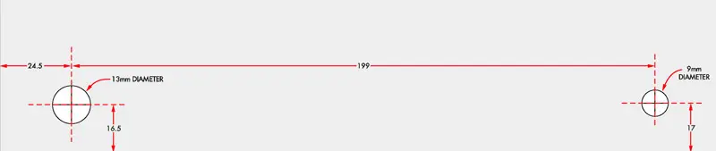
Fig.9: this drilling template for the rear panel can either be copied or downloaded in PDF format from the EPE website and printed out. Start each hole using a small pilot drill, then carefully enlarge it to the correct size using a tapered reamer.
Once these holes have been made, download and print out the rear-panel label from the EPE website. This can then be laminated and attached to the rear panel using silicone adhesive, after which the holes can be cut out using a sharp hobby knife.
The next step is to fit a 160 x 30mm piece of lmm-thick clear acrylic sheet over the front-panel display cut-out. This should be fitted from the rear and can be held in place by applying a thin smear of silicone sealant around the outside edge before attaching it to the panel.
The front and rear panels can now be attached to the main PCB. That’s done by first removing the mounting nuts from CON1 and CON3. Each panel is then fitted in place and the connector mounting nuts re-fitted. The rear panel simply fits over CON3, while the front panel not only fits over CON1 but also over CON2 and switches S1-S9.
Do the mounting nuts up finger-tight to hold things together, then lower the entire assembly into the bottom half of the case, with the panels slipping down inside the vertical moulded channels. Once it’s in place, the assembly can be fastened down using six 4G x 6mm self-tapping screws which go into integral pillars moulded into the case bottom with the connector nuts firmly tightened.
Mounting the display PCB
With the main assembly in place, you’re now ready to mount the display PCB. This is attached to the rear of the front panel using four M3 x 12mm tapped spacers and eight machine screws - see Fig.10. Note that M3 x 5mm screws are used to secure the spacers to the front panel, while M3 x 6mm screws are used to secure the display PCB to these spacers.
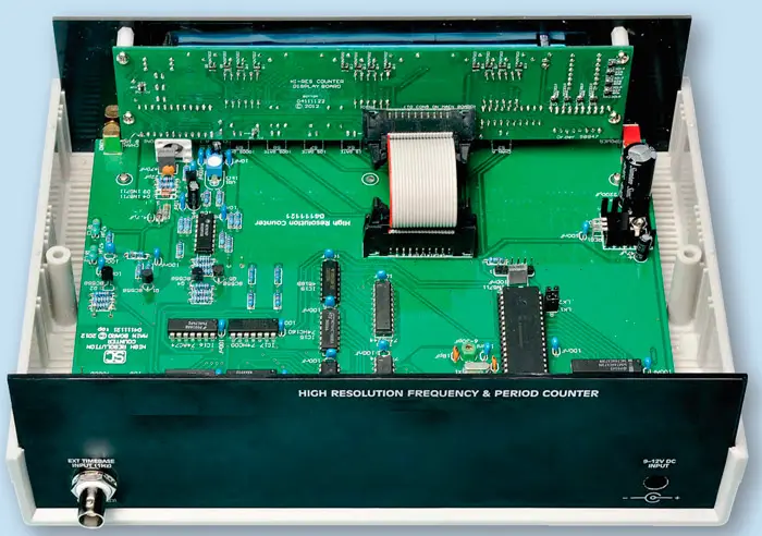
This is the view inside the completed 2.5GHz frequency counter, from the rear. All the parts fit on the main and display PCBs and these are linked together by a short IDC cable (see Figs.10 and 11). Power comes from a 9-12V DC 1A plugpack supply.
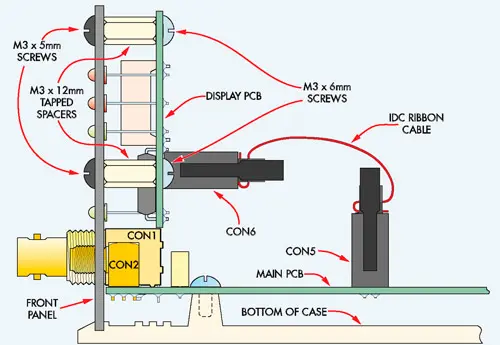
Fig.10: the mounting details for the two PCBs. The display PCB is attached to the front panel using M3 x 12mm tapped spacers and eight M3 screws (note the different lengths for the screws at each end of the spacers). This PCB assembly is then connected to the main PCB via a 20-way IDC cable (see Fig.11 for details).
The counter assembly can now be completed by making up and fitting the short IDC ribbon cable which links the two PCBs via CON5 and CON6.
Fig.11 shows how the IDC cable is made up. All you need is a 95mm length of 20-way flat ribbon cable plus the two 20-way IDC connectors. A small bench vice can be used to clamp the connectors in position if you don’t have an IDC crimping tool.
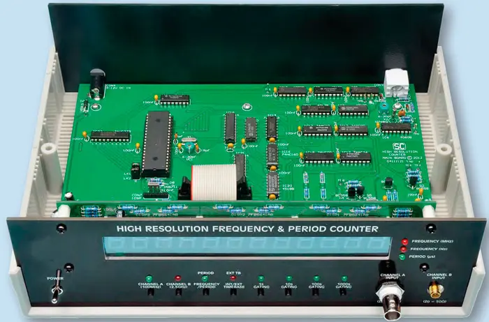
Another view of the completed frequency counter, this time from the front. The main PCB assembly is attached to the base of the case using six self-tapping screws that go into integral moulded pillars.
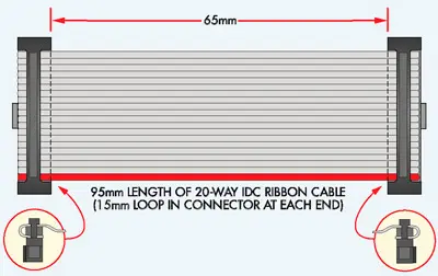
Fig.11: follow this diagram to make up the 20-way IDC cable. The cable is then used to link the main and display PCBs, as shown in Fig.10.
Don’t forget to fit the locking bar to each connector after crimping. The completed IDC cable is then used to link the two PCBs, as shown in Fig.10.
Set-up and adjustment
With the cable in place, the counter can now be powered up and adjusted.
Begin by connecting a 9-12V 1A DC plugpack supply to CON4 and then switch on using power-switch S1. You should immediately be greeted with the message ‘Silicon Chip’ on the 7-segment LED displays. In addition, the following indicator LEDs should light: LED4 (Channel A), LED8 (1s Gating) and LED2 (Frequency Hz).
The 7-segment displays should now show the initial message for a second or so, but then change to display just ‘0.’ on the extreme righthand digit, indicating that there is currently no input to channel A of the counter.
if the display shows something other than ‘0.’, this simply means that trimpot VR1 needs adjustment. In that case, use a small screwdriver to tweak VR1 in one direction or the other, until you get a zero display. Normally, this will be with VR1 set to about its midway position.
Next, check the Dc voltage at the output (rearmost) pin of REG1. It should be very close to +5.00V. You should also find this voltage at pins 1 and 16 of IC5, at TP3 and also pins 11 and 32 of PIC micro IC22.
Circuit changes
Since publication of Part 1 last month, we've changed a few component values and added two extra components, in order to achieve the highest possible performance from the counter. The details are as follows:
1) The capacitor in parallel with the 100kΩ resistor in the channel A input divider has been increased from 22pF to 47pF.
2) The 100μF electrolytic capacitor in parallel with the 10nF capacitor at Q3's source has been changed to a 47μF tantalum.
3) The resistors connecting pins 2 and 3 of IC5a to ground have been changed from 470Ω to 360Ω.
4) The resistor between pins 15 and 4 of IC5 has been changed from 1Ω to 680Ω.
5) A 100nF MKT capacitor has been added as a supply bypass between pins 1 and 16 of IC5 and ground.
6) A 56Ω resistor has been added between pin 4 of IC2 (and pin 27 of IC3) and the +3V (VL) supply line of the channel B prescaler. This is not shown in the photo of the prototype, but is included in the final version of the PCB.
7) To make it easier for the PIC's clock oscillator to be adjusted to exactly 8.000MHz with almost any crystal, the NP0 ceramic capacitor between pin 14 of IC22 and ground has been increased from 22pF to 39pF. Similarly, the capacitor in parallel with trimcap VC1 has been increased from 18pF to 27pF.
8) Tests with a number of 32.768kHz crystals in the internal timebase oscillator (IC6) have shown that, in some cases, it may be necessary to increase the fixed NPO ceramic capacitor from 39pF to 47pF, in order to achieve calibration.
Frequency calibration
Finally, you need to make two more adjustments involving trimcaps VC1 and VC2, which are used to calibrate the counter’s internal timebases. VC1 adjusts the PIC micro’s main 8MHz clock frequency from which the ‘1ps’ period counting timebase pulses are derived, while VC2 adjusts the frequency of the internal 1Hz timebase.
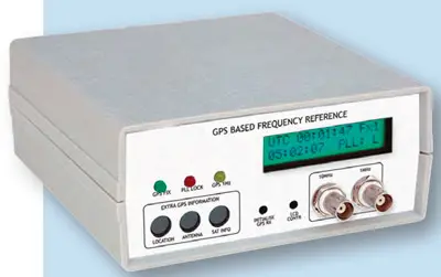
To make these adjustments, you’ll need a 1pps (ie, 1Hz pulses) signal from an accurate source like the GPS-Based Frequency Reference (EPE, April-May 2009). Here’s the procedure:
Switch the counter into its Period mode by pressing S4 and holding it down for half a second or so until LED6 lights. Then connect the accurate 1Hz signal from your GPS source to the counter’s channel A input. This should give you a display of close to ‘1000000’, which is the period of the 1Hz signal in microseconds. If the reading is slightly above or below this figure, carefully adjust VC1 until the reading is ‘1000000’.
The 1MHz ‘period clock’ that you’ve just calibrated is now used to adjust VC2, to calibrate the counter’s internal timebase. To do this, press S4 again and hold it down until LED6 goes out, showing that the counter has switched back to frequency mode.
Next, disconnect the GPS 1Hz signal from the Channel A input and instead connect a short coax test lead with insulated clips at its free end. Then connect the ‘live’ clip of this cable to TP2 at the rear centre of the counter’s main board (ignore the ‘earthy’ clip).
After making sure that LED7 is off (indicating that the counter is using its internal timebase), you should again get a reading that’s close to ‘1000000’, corresponding to the 1MHz ‘period measurement’ clock. If the reading you get is slightly above or below this correct figure, carefully adjust VC2 until the reading does become ‘1000000’.
This is using the default gating time of 1s, by the way. If you wish, you can switch to the 10s gating time by pressing S7 until LED9 lights. This will allow you to adjust VC2 until you get a reading of ‘1000000.0’, which is about as accurate as it’s possible to adjust the internal timebase.
Your counter will now be correctly set up and calibrated. All that remains is to fasten the top half of the case in position and the counter is ready for you to use.
Finally, if you don’t have access to the GPS-Based Frequency Reference, just set VC1 and VC2 to mid-range for the time being. We plan to describe a low-cost GPS-based 1pps reference in the near future, so this can be used for calibration at a later date.
You’ll need the GPSBased Frequency Reference (EPE, April-May 2009) to accurately calibrate the unit (or some other accurate 1pps signal source). We will describe a low-cost GPS 1pps reference in the near future.
Parts List - Frequency Counter
1 front panel PCB, available from the EPE PCB Service, coded 04111123
1 plastic instrument case, 256mm x189mm x 83mm
1 9-12V DC 1A plugpack
1 95mm length of 20-way IDC ribbon cable
2 20-way IDC line sockets
6 4G x 6mm self-tapping screws
4 rubber self-adhesive feet
1 160 x 30mm clear acrylic sheet (1mm thick)
Main PCB
1 PCB, available from the EPE PCB Service, coded 04111121, size 225mm x 175mm
1 8.00MHz crystal, HC-49 (X1)
1 32.768kHz crystal, DT38 case (X2)
2 47μH RF chokes, axial type (RFC1,RFC2)
1 wideband SHF choke, SMD type (Mini-Circuits ADCH-80A+) (RFC3)*
1 40-pin 0.6-inch DIL IC socket 1 small finned TO-220 heatsink, 19mm square
1 SPDT mini toggle switch, 90° PCB-mount (S1)
8 SPST micro tactile switches, 90° PCB-mount with 6mm or longer actuators (S2-S9)
2 BNC sockets, PCB-mount (CON1, CON3)
1 SMA reverse pCb socket, 90° (CON2) F
1 2.5mm concentric DC socket, PCB-mount (CON4)
1 6-pin SIL header (ICSP connector)
1 20-way IDC locking header (CON5)
2 2-pin SIL headers
2 2-way jumper shunts
10 1mm-diameter PCB stakes
1 M3 x 6mm machine screw
1 M3 nut
1 1kΩ mini horizontal trimpot (VR1)
Semiconductors
1 ERA-2SM+ wideband monolithic amplifier (IC1)*
1 MC12095 ECL microwave frequency divider, SOIC (IC2) LD
1 MC10E016 ECL synchronous mod-16 UHF counter, PLCC (IC3) LD
1 MC10EL32 ECL UHF flip-flop, SOIC (IC4) F
1 MC10116P ECL triple line receiver (IC5) LD
1 4060B CMOS counter (IC6)
3 4518B CMOS dual BCD counters (IC7,IC9,IC20)
2 4093B CMOS quad Schmitt NANDs (IC8,IC10)
1 4012B CMOS dual 4-input NAND (IC11)
1 74AC10 high-speed CMOS triple 3-input NAND (IC12) F
2 74AC00 high-speed CMOS quad 2-input NANDs (IC13, IC15) F
1 74AC163 high-speed CMOS synchronous mod-16 counter (IC14)
1 74HC160 CMOS synchronous BCD decade counter (IC16)
1 74AC74 high speed dual D-type flip-flop (IC17) F
1 74HC00 CMOS quad 2-input NAND (IC18)
2 74HC244 CMOS octal buffer/line drivers (IC19,IC21)
1 PIC16F877A MCU programmed with 0411112A.hex (IC22)
1 74HC373 CMOS octal latch (IC23) 1 74HC161 CMOS synchronous mod-16 counter (IC24)
1 7805 +5V regulator (REG1)
4 BC558 PNP transistors (Q1,Q2, Q4,Q5)
1 2N5485 VHF junction FET (Q3) LD
2 NX2301P P-channel MOSFETs (Q6,Q7) F
1 3.3V 1W Zener diode (ZD1)
2 1PS70SB82 very high speed Schottky diodes (D1,D2) F
3 1N5711 Schottky diodes (D3,D4, D8) F
2 1N4148 signal diodes (D5,D6)
1 1N5819 1A Schottky diode (D7)
Capacitors
1 2200μF 25V RB electrolytic
1 47μF 16V tantalum
1 47μF 16V RB electrolytic
1 10μF 16V RB electrolytic
1 4.7μF 25V tantalum
1 470nF MKT
2 100nF MKT
6 100nF X7R MMC 1206 SMD F
25 100nF through-hole MMC
4 10nF X7R MMC 1206 SMD F
5 10nF through hole MMC
2 1nF C0G MMC 1206 SMD F
2 47pF NP0 disc ceramic 1 39pF NP0 disc ceramic
1 27pF NP0 disc ceramic
2 6-30pF mylar mini trimcaps (VC1,VC2)
Resistors (0.25W, 1%)
1 10MΩ | 2 360Ω |
1 910kΩ | 1 180Ω |
1 220kΩ | 1 120Ω |
3100kΩ | 2 100Ω 0805 SMD F |
1 22kΩ | 1 82Ω |
1 10kΩ | 1 75Ω |
1 2.2kΩ | 1 56Ω |
3 1kΩ | 3 51Ω |
1 680Ω | 1 47Ω 0805 SMD F |
9 470Ω | 2 27Ω |
1 430Ω |
Display PCB
1 PCB, available from the EPE PCB Service, coded 04111122, size 200mm x 50mm
1 20-way IDC locking header (CON6)
4 M3 x 12mm tapped Nylon spacers
4 M3 x 6mm machine screws
4 M3 x 5mm machine screws
Semiconductors
3 7FB5641AB quad 7-segment blue LED displays (DISP1, DISP2,DISP3) (Futurlec)*
1 74HC240 CMOS octal buffer/line driver (IC25)
1 4514B CMOS 1-16 latching decoder (IC26)
15 2N7002 N-channel MOSFETs (Q8-Q22) F
8 NX2301P P-channel MOSFETs (Q23-Q30) F
4 3mm red LEDs (LED1, LED2, LED5, LED7)
7 3mm green LEDs (LED3, LED4, LED6, LEDs8-11)
Capacitors
1 100μF 16V RB electrolytic
2 100nF through-hole MMC
Resistors (0.25W, 1%)
7 220Ω 8 47Ω 23 27QΩ
1 10kΩ SIL resistor array, 8x or 9x F
The programmed PIC microcontroller and parts marked with a red asterisk (*) are available from the Silicon Chip Partshop: www.siliconchip.com.au/ shop. Parts marked with an F are available from Farnell. Parts marked LD are available from: www.littlediode.com
Note: Do ensure all parts are available before commencing project
Author: Jim Rowe