
Electronics News
Archive : 20 July 2015 год
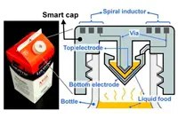 Engineers at the University of California, in collaboration with colleagues at Taiwan's National Chiao Tung University, have integrated electrical components, such as resistors, inductors, capacitors and integrated wireless electrical sensing systems into the 3D printing process. They have put the new technology to the test by printing a wireless 'smart cap' for a milk carton that detects signs of spoilage using embedded sensors.
"Our paper describes the first demonstration of 3D printing for working basic electrical components, as well as a working wireless sensor," said senior author Liwei Lin, a professor of mechanical engineering and co-director of the Berkeley Sensor and Actuator Centre.
Polymers are used in 3D printing because their flexibility allows them to be formed into a variety of shapes. However, they are poor conductors of electricity. To get around this, the researchers built a system using polymers and wax. They then removed the wax, leaving hollow tubes into which liquid metal was injected and then cured.
The shape and design of the metal determined the function of different electrical components. For instance, thin wires acted as resistors, and flat plates were made into capacitors.
The researchers integrated the electronic components into a plastic milk carton cap to monitor signs of spoilage. The 'smart cap' was fitted with a capacitor and an inductor to form a resonant circuit. A flip of the carton allowed a bit of milk to get trapped in the cap's capacitor gap, and the carton was then left unopened at room temperature for 36 hours.
The circuit detected the changes in electrical signals that accompany increased levels of bacteria. The researchers monitored the changes with a wireless radio-frequency probe at the start of the experiment and every 12 hours thereafter, up to 36 hours. The smart cap found that the peak vibration frequency of the room-temperature milk dropped by 4.3% after 36 hours. In comparison, a carton of milk kept at 4°C saw a relatively minor 0.12% shift in frequency over the same time period.
"This 3D-printing technology could eventually make electronic circuits cheap enough to be added to packaging to provide food safety alerts for consumers," Prof Lin said. "You could imagine a scenario where you can use your cellphone to check the freshness of food while it's still on the store shelves."
Lin said his lab is working on developing this technology for health applications, such as implantable devices with embedded transducers that can monitor blood pressure, muscle strain and drug concentrations.
Author
Tom Austin-Morgan
Source: www.newelectronics.co.uk
 In a move which broadens its support for processor core debug, UltraSoC has added Cadence's Tensilica Xtensa family to its UltraDebug package.
"UltraSoC has innovative technology when it comes to SoC debug," said Chris Jones, product marketing group director of the Tensilica division of the IP Group at Cadence. "Its technology helps designers to create competitive products quickly and we're looking forward to working together to solve the SoC debug challenge, which we believe is one of the challenges facing the semiconductor industry today."
Rupert Baines, UltraSoC's CEO, added: "Today's application processors are not optimised to handle the vast range of tasks required in today's advanced consumer products – in particular, datapath processing. Xtensa technology provides a solution to that problem, offloading tasks from the host processor and creating highly optimised multicore SoCs. We're very much in tune with this vision of the SoC and delighted to be working with an industry leader like Cadence to make it happen."
Xtensa enables system architects to create high performance processors and DSPs customised to their application needs. This is said to allow the creation of SoCs in which key tasks are offloaded from the host processor to multiple heterogeneous Xtensa processors.
Author
Graham Pitcher
Source: www.newelectronics.co.uk
 As part of the £100million for research into intelligent mobility announced by the Chancellor in the Spring 2015 Budget, the government has launched a £20m competitive fund for collaborative research and development into driverless vehicles, along with a code of practice for testing.
The measures announced by Business Secretary Sajid Javid and Transport Minister Andrew Jones will put the UK at the forefront of the intelligent mobility market, expected to be worth £900billion by 2025.
Business Secretary Sajid Javid said: "Our world beating automotive industry, strengths in innovation and light touch regulatory approach to testing driverless technology combine to make the UK market competitive and an attractive destination for investors."
The government wants bidders to put forward proposals in areas such as safety, reliability, how vehicles can communicate with each other and the environment around them and how driverless vehicles can help give an ageing population greater independence.
Transport Minister Andrew Jones said: "Driverless cars will bring great benefits to our society and economy and I want the UK to lead the way in developing this exciting technology. Our code of practice clearly shows that the UK is in the best position when it comes to testing driverless cars and embracing the motoring of the future. We now look forward to working with industry to make this a reality."
The code of practice provides industry with the framework they need to safely trial cars in real-life scenarios, and to create more sophisticated versions of the models that already exist.
The Department for Transport and Department for Business, Innovation and Skills have established the new joint policy unit, the Centre for Connected and Autonomous Vehicles (C-CAV), which will co-ordinate government policy on driverless cars and connected technology. C-CAV is currently working on a range of new technological developments, including plans to test new roadside communication technology to improve traffic flow and safety through 'connected corridors'. This would pilot technology that will provide drivers with useful journey and safety information.
Author
Tom Austin-Morgan
Source: www.newelectronics.co.uk
 Researchers from North Carolina State University and Brown University have found that zinc oxide and silicon nanowires have a pronounced anelasticity. This could enable the development of stretchable, flexible wearable devices.
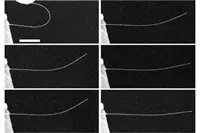
It was found that – when bent – the nanowires would return more than 80% of the way to their original shape instantaneously, but return the rest of the way (up to 20%) slowly.
"All materials have some degree of anelasticity, but it is usually negligible at the macroscopic scale," says Yong Zhu, associate professor of mechanical and aerospace engineering at NC State and author of a paper describing the work. "Because nanowires are so small, the anelasticity is significant and easily observed - although it was a total surprise when we first discovered the anelasticity in nanowires."
The anelasticity was discovered when Zhu and his students were studying the buckling behaviour of nanowires.
"Anelasticity is a fundamental mechanical property of nanowires, and we need to understand these sorts of mechanical behaviours if we want to incorporate nanowires into electronics or other devices," says Elizabeth Dickey, a professor of materials science and engineering at NC State and co-author of the paper. Nanowires hold promise for use in a variety of applications, including flexible, stretchable and wearable electronic devices.
When any material is bent, the bonds between atoms are stretched or compressed to accommodate the bending, but in nanoscale materials there is time for the atoms to also move, or diffuse, from the compressed area to the stretched area in the material. If you think of the bent nanowire as an arch, the atoms are moving from the inside of the arch to the outside. When the tension in the bent wire is released, the atoms that simply moved closer or further apart snap back immediately; this describes elasticity. But the atoms that moved out of position altogether take time to return to their original sites. That time lag is a characteristic of anelasticity.
"This phenomenon is pronounced in nanowires. For instance, zinc oxide nanowires exhibited anelastic behaviour that is up to four orders of magnitude larger than the largest anelasticity observed in bulk materials, with a recovery time-scale in the order of minutes," says Huajian Gao, a professor at Brown University and co-corresponding author of the paper.
Detailed modelling by Gao's group indicates that the pronounced anelasticity in nanowires is because it is much easier for atoms to move through nanoscale materials than through bulk materials. And the atoms don't have to travel as far. In addition, nanowires can be bent much further than thicker wires without becoming permanently deformed or breaking.
The team plans to explore whether this pronounced anelasticity is common across nanoscale materials and structures. They also want to evaluate how this characteristic may affect other properties, such as electrical conductivity and thermal transport.
Pic: Time lapse image: Top left, the image shows a nanowire bent almost in half, and then 5 seconds after release (middle left), 10 seconds (bottom left), 60 seconds (top right), 10 minutes (middle right), and 20 minutes (bottom right) after release.
Author
Tom Austin-Morgan
Source: www.newelectronics.co.uk
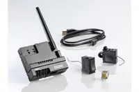 RS Components (RS) claims it is making energy-harvesting applications easier and faster to develop with the Wireless Switch Evaluation Kit and modular snap and rocker switches by Cherry.
The AFIK-1002 evaluation kit is said to contain everything needed to setup wireless links using self-powered switches, and to test key parameters such as signal strength and range in custom applications. The kit includes an energy-harvesting generator, a snap switch, a rocker switch, a receiver with antenna bushing, a USB cable and an operating manual. Additionally, the components are available to purchase individually from RS, enabling designers to create their own wireless switch.
"RS has a large customer base that is closely matched to our target market, typically engineers needing an easy-to-use and totally independent solution to remote-control challenges," said Mark Mills, European distribution manager at Cherry.
Self-powered 868MHz snap and rocker switches, as well as an 868MHz receiver module, are also available. The switches transmit at low power, typically 10 to 14dBm, and up to 100kbit/s. Each has a unique 32-bit identification, allowing several switches to be paired with one receiver or one switch with several receivers.
The receiver is available as a board or as a complete module. Multiple outputs including a TTL output, low-voltage relay output, and RS-232 and RS-485 bus outputs allow the unit to be connected to various types of equipment.
Author
Tom Austin-Morgan
Source: www.newelectronics.co.uk
 TSMC hasn't given up hope on using EUV lithography at the 10nm node, but it appears to be more likely to be introduced at the 5nm node. Speaking on a conference call, Mark Liu, TSMC's president and co-CEO, pictured, said: "We are planning to exercise EUV at 7nm and are currently planning to use EUV at 5nm. But it depends on certain development criteria and milestones."
He added that TSMC's assessment of the technology shows that EUV will reduce the number of masking layers needed at 5nm and provide better control.
Despite recently selling its shareholding in ASML, TSMC continues to work closely with the tools developer. "We have made very good progress on source power," Liu continued, "as well as on photoresists. However, the current challenge is more on the masks and we are working with ASML."
Author
Graham Pitcher
Source: www.newelectronics.co.uk
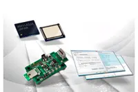 Renesas Electronics has developed the RL78/G1D Group of MCUs that combines Bluetooth Low Energy technology with the RL78 MCU. The MCUs are claimed to Extend Battery Life and simplify circuit design.
The current consumption of the RL78/G1D is claimed to be the lowest in the industry at 3.5mA during reception and 4.3mA during transmission. Adaptable RF technology adjusts the power consumption during wireless operation to the optimal level to match the communication distance.
The MCUs are also claimed to simplify Antenna Circuit Design by integrating on-chip balun elements that otherwise would have to be provided in an external antenna connection circuit. They are also claimed to extend the battery life of embedded IoT devices.
An evaluation kit and Bluetooth-SIG qualified protocol stack, allows system designers to conduct evaluation of wireless characteristics and initial evaluation of communication behaviors. The MCUs are provided with PC GUI tool for manipulation of these components.
Author
Tom Austin-Morgan
Source: www.newelectronics.co.uk