
Electronics News
Archive : 28 July 2015 год
 Researchers from North Carolina's Duke University have developed an ultrafast light-emitting device that can flip on and off 90billion times a second and could form the basis of optical computing.
In a study, a team from the Pratt School of Engineering pushed semiconductor quantum dots to emit light at more than 90GHz. This so-called plasmonic device could one day be used in optical computing chips.
"This is something that the scientific community has wanted to do for a long time," said Maiken Mikkelsen, assistant professor of electrical and computer engineering and physics at Duke. "We can now start to think about making fast-switching devices based on this research."
When the researchers shone a laser on the surface of a silver cube 75nm wide, the free electrons on its surface began to oscillate together in a wave. These oscillations create their own light, which reacts with the free electrons. Energy trapped on the surface of the nanocube in this fashion is called a plasmon.
The plasmon creates an intense electromagnetic field between the silver nanocube and a thin sheet of gold placed 20 atoms away. This field interacts with quantum dots that are sandwiched between the nanocube and the gold. The quantum dots, in turn, produce a directional, efficient emission of photons that can be turned on and off at more than 90GHz.
"There is great interest in replacing lasers with LEDs for short-distance optical communication, but these ideas have always been limited by the slow emission rate of fluorescent materials, lack of efficiency and inability to direct the photons," said Gleb Akselrod, a postdoctoral researcher in Mikkelsen's laboratory. "Now we have made an important step towards solving these problems."
The group is now working to use the plasmonic structure to create a single photon source - a necessity for secure quantum communications - by sandwiching a single quantum dot in the gap between the silver nanocube and gold foil. They are also trying to precisely place and orient the quantum dots to create the fastest fluorescence rates possible.
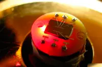
Pic: A nanoscale view of the superfast fluorescent system using a transmission electron microscope. The silver cube is 75nm wide. The quantum dots (red) are sandwiched between the silver cube and a thin gold foil.
Author
Tom Austin-Morgan
Source: www.newelectronics.co.uk
 Due to an overwhelming demand to extend the submission date for the British Engineering Excellence Awards (BEEAs) entries, Friday 7th August has been chosen as the new deadline for entries.
The Awards recognise companies and individuals who have excelled in design engineering within the last year. Receiving one of these prestigious awards provides great publicity, and opens doors for future success and growth.
The judges for the BEEAs are drawn from a cross section of electronic and engineering design disciplines, and are highly qualified.
There are 10 categories to enter, demonstrating the depth and quality of UK engineering design. Categories include Design Engineer of the Year, Green Product of the Year, Mechanical Product of the Year and Start-Up of the Year.
The deadline for entries is now 7th August 2015 and the winners will be announced at a gala lunch at the Hurlingham Club, London, on 29th October. Entry is free and all the categories and entry criteria can be found here.
Author
Tom Austin-Morgan
Source: www.newelectronics.co.uk
 A research team from the University of Pennsylvania has demonstrated a silicon based photonic device that is sensitive to the spin of the photons in a laser shined on one of its electrodes. According to the team, light that is polarised clockwise causes current to flow in one direction, while anticlockwise polarised light makes it flow in the other direction.
The property is said to be a function of the geometric relationship between the pattern of atoms on the surface of silicon nanowires and how electrodes placed on those wires intersect them. The interaction between the semiconducting silicon and the metallic electrodes produces an electric field at an angle that breaks the mirror symmetry that silicon typically exhibits, sending electrons in one direction or the other down the nanowire.
Professor Ritesh Agarwal said: "Whenever you change a symmetry, you can do new things. In this case, we have demonstrated how to make a photodetector sensitive to a photon's spin. All photonic computers need photodetectors, but they currently only use the quantity of photons to encode information. This sensitivity to photon spin would be an extra degree of freedom, meaning you could encode additional information on each photon.
"Typically, materials with heavy elements show this property due to their spins strongly interacting with electron's orbital motion. But we have demonstrated this effect on the surface of silicon, originating only from the electron's orbital motion."
Prof Agarwal's team is now working on ways to get planar silicon to exhibit these properties using the same mechanism.
Author
Graham Pitcher
Source: www.newelectronics.co.uk
 More than 70 school students from the UK, Ireland, Romania and Greece will be taking part in the University of Southampton's Electronics and Computer Science (ECS) annual summer school, which starts on Monday 27 July.
Dr Geoff Merrett, senior admissions tutor for ECS, said: "We hope that, by taking part in the summer school, we have engaged the students in the subjects, inspired them to apply for a university place and opened their eyes to the exciting breadth of careers a degree in ECS can lead to."
Students will attend lectures covering topics ranging from electronic and electrical engineering to computer science and software engineering and be able to visit the University's specialist facilities, such as the Tony Davies High Voltage Laboratory and the Southampton Nanofabrication Centre.
Alongside offering students a taste of university study through lectures, lab work and group challenges, the event will help them to better understand career options for electronics graduates with a day trip to the event sponsors – JP Morgan and Imagination Technologies. This will show them how electronics and computer science skills are applied in business and industry.
The students will also be working on a team challenge before giving presentations at a prize giving ceremony on 31 July.
Pic: Dr Geoff Merrett, senior admissions tutor for ECS
Author
Graham Pitcher
Source: www.newelectronics.co.uk