
Electronics News
Archive : 22 September 2015 год
 Analogue and sensor specialist ams is looking to become a €1billion company by 2019, according to CEO Kirk Laney,who will be succeeed by Alexander Everke in March 2016.
The company has seen a significant increase in revenue this year, with Q2 profit up by 59% to €170m, compared to Q2 2014, while H1 profit is up by 68% to €323m. Revenue has been buoyed by the continued growth of the Asian market, specifically China, and the company’s shift towards producing sensors for consumer products. According to ams, 71% of the sensors it now produces are for the consumer market, mainly smartphones and other mobile devices.
“We have a very good position in the mobile space,” Laney said. “We have our foot in the door with mobile suppliers and have expended into audio, near field communication and optical sensors for mobile devices. As long as the bottom line looks good, we could go 100% consumer.”
The consumer market in Asia has increased significantly in the last year, representing 65% of ams’ business in the first half of 2015 compared to 48% at the same point in 2014. However, Laney said: “The Asian market is getting more cautious and orders are becoming less predictable.”
In an effort to expand into the American market, which currently contributes 4% of revenue, ams is building a fab in New York State. The fab, being built to ams’ specifications, will be leased to the Austrian company for the next 20 years, meaning it will suffer no depreciation whilst reaping significant cost-per-wafer benefits.
Chief operating officer Dr Thomas Stockmeier said: “Building a new wafer fab will help us achieve our growth plans and meet increasing demand for our advanced manufacturing nodes.
“Our decision to locate the facility in New York was motivated by the highly skilled workforce, the proximity to esteemed education and research institutions, and the favourable business environment provided by Governor Cuomo (Governor of New York) and the public and private partners we are working with on this important project.”
Laney added: “Our infrastructure in Austria is maxed out and opportunities were better in the US than Asia. We fit a hole it was looking to fill in sensor technologies.”
Its Austrian fab produces some 180,000 200mm wafers per year and has no room to expand production. The New York fab is expected to produce 150,000 200mm wafers in its first buildout with the capability for a 130nm manufacturing process. The eventual manufacturing capacity is estimated to be around 450,000 200mm-equivalent wafers per annum.
As well as consumer and communications devices and more challenging applications in the automotive, medical and industrial industries, ams is targeting the Internet of Things, especially smart homes and working environments.
People’s circadian timing can be influenced by smart sensors that modify the light spectrum on a nonphotic level. This can be used in the home to promote better sleep patterns, while better LED lighting in factories and offices could have an impact on mood and productivity.
The smart lighting technology is based on XML coding and as such can be added to without having to upgrade software or replacing obsolete units. Atmospheric sensors, powered by the light fixture, can be added to the system, enabling features like temperature and ventilation to be optimised.
Pic: Kirk Laney, CEO of ams
Author
Tom Austin-Morgan
Source: www.newelectronics.co.uk
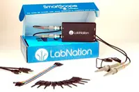 Following a successful Kickstarter campaign, Belgian company LabNation has launched SmartScope, an open source USB test equipment package said to be the first such system designed to run on multiple operating systems and platforms.
Chief technology officer Riemer Grootjans said SmartScope is targeted at a new range of users. “Development has been pushed by the appearance of boards like Raspberry Pi and Arduino,” he said. “More people are becoming involved in electronics and they need test and measurement tools. But they’re not designing in things like DDR3, so don’t need GHz performance.”
SmartScope offers oscilloscope, logic analyser and waveform generator functionality in a package measuring 110 x 64 x 24mm. The device, along with probes, wires and cables, will sell for €229.
The oscilloscope provides two analogue channels sampling at up to 100Msample/s and with a -3dB bandwidth of 30MHz. The eight channel logic analyser has a user selectable logic level of 3.3 or 5V DC, while the single channel waveform generator can create arbitrary waveforms with a data rate up to 50Msample/s and an output level from 0 to 3.3V. A four channel digital output generator runs at up to 100Msample/s at either 3.3 or 5V.
Author
Graham Pitcher
Source: www.newelectronics.co.uk
![]() Internet of Things applications, such as connected cars, wearable electronics and building automation, are boosting demand for microcontrollers. According to the latest Microcontroller Market Tracker report from market analyst IHS, sales of MCUs into IoT applications is expected to grow from $1.7billion in 2014 to $2.8bn in 2019. By contrast, the overall MCU market is expected to grow at 4% a year until 2019.
Internet of Things applications, such as connected cars, wearable electronics and building automation, are boosting demand for microcontrollers. According to the latest Microcontroller Market Tracker report from market analyst IHS, sales of MCUs into IoT applications is expected to grow from $1.7billion in 2014 to $2.8bn in 2019. By contrast, the overall MCU market is expected to grow at 4% a year until 2019.
“What some still consider to be only hype surrounding emerging IoT trends has already begun disrupting the MCU market,” said Tom Hackenberg, senior analyst for IHS Technology. “In fact, without the influence of IoT application growth, the MCU market is predicted to stagnate by the end of the decade.”
However, Hackenberg noted the industry’s challenge is to quantify this new opportunity. “IoT is a conceptual trend, not a device, application or even a new feature,” he said. “Suppliers must therefore focus on their target markets and concentrate on the specific values they bring to these markets.”
Author
Graham Pitcher
Source: www.newelectronics.co.uk
 Researchers at the University of Twente have demonstrated working electronic circuits produced using methods which they say resemble Darwinian evolution.
The team has moved away from conventionally designed circuits, using instead an approach that resembles those found in nature. By using such a ‘designless’ approach, the team says costly design mistakes can be avoided.
An artificial evolution approach is said to take less than an hour. By applying electrical signals, a network can be configured into 16 different logical gates, with the approach working around – or even taking advantage of – possible material defects that could be fatal in conventional electronics.
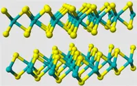
A schematic of a nanoparticle network, about 200nm in diameter, is shown in the image. By applying electrical signals at the electrodes (yellow) and using an artificial evolution technique, this disordered network of gold nanoparticles can be configured into useful electronic circuits.
The team says it is the first time this approach has been used to create electronics with dimensions that compete with commercial technology. According to Professor Wilfred van der Wiel, the circuits have limited computing power. “But with this research we have delivered proof of principle and demonstrated that our approach works in practice. By scaling up the system, real added value will be produced in the future.”
A potential advantage for this type of circuitry is that it might require much less energy to manufacture and during use.
The researchers anticipate a wide range of applications, for example in portable electronics and in the medical world.
Author
Graham Pitcher
Source: www.newelectronics.co.uk
 An MIT-led group of researchers has claimed to have determined a way to make large sheets of molybdenum telluride. The team says their method is also likely to work for many similar 2D materials, and could make widespread applications in electronics feasible.
“This material has a similar bandgap to silicon and in single-layer form it has a direct bandgap,” said Lin Zhou, MIT postdoctoral researcher. “It also has strong absorption for solar radiation.” This makes Molybdenum telluride (MoTe2) key to making solar cells and transistors and it also lends itself to applications in spintronics.
MoTe2 can exist in two different forms; one is metallic, meaning it conducts electricity well, and the other is a natural semiconductor, lending itself to applications in electronics. Controlling how the material is made allows the researchers to create whichever form is needed for a particular use.
The method of creating these large sheets is based on chemical vapour deposition (CVD), and makes it possible to create sheets of any thickness, and of a size limited only by the dimensions of the CVD chamber used for deposition.
One challenge the team had to overcome was that the atoms of molybdenum telluride are weakly bound to each other, so the tendency of the two precursor materials to form molybdenum telluride is low.
The researchers were able to overcome this by using several stages of deposition, beginning with a layer of pure molybdenum. “This method makes it easy, because you only need to control one material,” Zhou explained. This step is followed by oxidation of that layer; this material is then removed and powdered tellurium is added, vaporised in a carrier gas of hydrogen and argon, at a temperature of 700°C. The use of hydrogen in the process, the team found, is crucial to producing a uniform MoTe2 film.
“Our process can grow sheets that have a very large area, are very homogeneous, and have high quality,” Zhou added.
The team now aims to explore adapting this process to create large sheets of other promising thin materials.
Author
Tom Austin-Morgan
Source: www.newelectronics.co.uk
 Dialog is to acquire Atmel in a cash and stock transaction that values the latter at $4.6bn. According to Dialog, the deal will create a global leader in power management and embedded processing solutions.
According to Dialog’s CEO Jalil Bagherli, pictured, the rationale for the deal is clear. “The potential this combination holds is exciting. By bringing together our technologies, world class talent and broad distribution channels we will create a new, powerful force in the semiconductor space.”
The combined company is looking to become a leader in the mobile power, IoT and automotive sectors. “This is an important and proud milestone in the evolution of our story,” Bagherli added.
Dialog is already a market leader in the power management sector and will acquire a portfolio of proprietary and ARM based microcontrollers, as well as devices for connectivity, touch and security.
“Adding Dialog’s capabilities in power management with Atmel’s keen focus on microcontrollers, connectivity and security will enable Dialog to more effectively target high-growth applications within the Mobile, IoT and Automotive markets,” claimed Steven Laub, Atmel’s president and CEO.
Author
Graham Pitcher
Source: www.newelectronics.co.uk