
Electronics News
Archive : 8 January 2016 год
 Organic LEDs are attractive not only because they emit light in all observation directions, but also for their colours and high contrast. It is also possible to manufacture transparent and flexible OLEDs, enabling new applications.
OLEDs consist of ultra thin layers of organic materials – the emitter – between two electrodes. When a voltage is applied, electrons from the cathode and holes from the anode are injected into the emitter, where they form electron-hole pairs, or excitons, which release energy when they decay.
Excitons have two states: singlet excitons decay immediately and emit light, whereas triplet excitons release their energy in the form of heat. To enhance the energy efficiency of an OLED, triplet excitons are used to generate light. Conventional LEDs use heavy metals, such as iridium and platinum, for this purpose, but these materials are expensive, have a limited availability and require complex production methods.
According to the team, it is cheaper and more environmentally friendly to use copper complexes as emitter materials. A process known as thermally activated delayed fluorescence (TADF) ensures high light yields and, hence, high efficiency.
TADF is based on the quantum mechanics phenomenon of intersystem crossing (ISC) and, for the first time, the speed of ISC has been measured in a highly luminescent solid state TADF copper(I) complex. The researchers – from Karlsruhe Institute of Technology, OLED manufacturer Cynora and the University of St Andrews – the transition from singlet to triplet took 27ps, whilst the reverse process saw a TADF of 11.5µs.
The researchers say these measurements should help to improve the understanding of mechanisms which lead to TADF, as well as contributing to the specific development of TADF materials for use in energy efficient OLEDs.
Author
Graham Pitcher
Source: www.newelectronics.co.uk
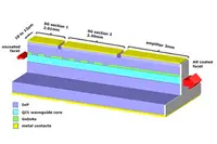 A team from Northwestern University in the US claims it has made the laser simpler and more versatile by integrating a mid infrared tunable laser with an on chip amplifier. The development is said to allow an adjustable wavelength output, modulators and amplifiers to be held inside a single package.
According to the team, the laser has demonstrated an order of magnitude more output power than its predecessors, while the tuning range has been enhanced by more than 100%.
“We have always been a leader in high-power and high-efficiency lasers,” said Professor Manijeh Razeghi. “Combining an electrically tunable wavelength with high power output was the next logical extension.”
Mid-infrared spectroscopy allows chemicals to be identified through their unique absorption spectra. This enables the detection of hazardous chemicals or possible explosives. Because Prof Razeghi’s system is also directional, the high power can enhance the ability to detect chemicals. The technology could also find application in free space optical communications and aircraft protection, says the team.
Author
Graham Pitcher
Source: www.newelectronics.co.uk
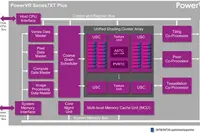 Imagination Technologies has extended its Rogue graphics architecture with the addition of two GPUs. The devices, part of the PowerVR Series7XT Plus family, are said to be aimed at the premium and mid-range segments of the consumer electronics market.
Peter McGuinness, director of multimedia technology marketing, said: “We’re rolling out new GPUs with high system efficiency and performance to support user experiences related to computational photography, computer vision, virtual reality, augmented reality and other advanced visual experiences – all while extending battery life.”
The GT7200 Plus is a dual-cluster configuration with 64 ALU cores, while the quad cluster GT7400 Plus has 128 ALU cores. Both designs are said to retain the features found in other Series7XT devices, but can take advantage of a new integer pipeline for vision related applications and added hardware support for the OpenCL 2.0 compute API.
The company also says that it has updated the microarchitecture to boost system performance and reduce power consumption. These goals have been achieved by proving support for the latest bus interfaces, doubling memory burst sizes and tuning the size of cache memories whilst improving their efficiency.
Author
Graham Pitcher
Source: www.newelectronics.co.uk
 The Centre for Process Innovation (CPI) and Beneq have signed a long term collaboration agreement for the use of atomic layer deposition (ALD) technologies in printable electronics applications.
The agreement brings together Beneq’s high precision vacuum coating alongside CPI’s capability in the scale up of printed electronics. Working together, the two organisations say they will provide world leading capability for the commercialisation of ALD techniques, creating an open access environment for companies to develop ultra barrier solutions in photovoltaics, Organic Light Emitting Diodes (OLEDs), microelectronics and sensors.
Alf Smith, business development manager at CPI, said: “The partnership between Beneq and CPI means that we will be able to constantly refine and optimise our capability and associated processes over the coming years to ensure that we remain a world leader in ALD coatings.”
ALD is applied as a specialist barrier coating technique used for the protection of optoelectronic devices and is being utilised by CPI to add moisture ultra-barrier protection layers to flexible polymer substrates used to produce optoelectronic devices using sensitive active electronic materials.
Thin films produced using the ALD method are said to be cost efficient, defect free and completely conformal, thus providing superior barriers and surface passivation compared with other deposition techniques. These properties suit them for applications that utilise flexible films such as OLEDs, flexible display screens, photovoltaic cells and wearable electronics amongst others.
Current commercial barrier films, based on multilayer laminates are typically prohibitively expensive for large area applications while single thin layer barrier structures from ALD deposition are claimed to have demonstrated the potential to reduce this cost whilst retaining the requisite barrier and flexibility properties.
Dr Mikko Söderlund, head of industrial solutions at Beneq added: “Beneq and CPI share a vision of the enabling role of ALD in flexible electronics. Pilot-scale operation and rapid prototyping with our equipment provides Beneq with invaluable information on system performance, and our customers benefit from an established R&D platform and faster time to market with ALD applications.”
The agreement follows CPI’s recent installation of two atomic layer deposition tools from Beneq for the development of conformal nano-scale coatings; one batch ALD tool and one state of the art roll-to-roll ALD (R2R ALD) system.
Further application areas of ALD and R2R ALD will be developed during the collaboration, where conformal nano-scale coatings are beneficial which would include transport, interfacial and contact layers in devices such as OLEDs, PV and sensors.
Author
Tom Austin-Morgan
Source: www.newelectronics.co.uk
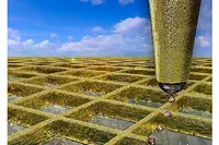 Researchers at ETH Zurich have used a 3D print technology called Nanodrip to create a new type of transparent electrode, which takes the form of a grid made of gold or silver ‘nanowalls’ on a glass surface.
The electrode is to have a higher conductivity and to be more transparent than those made of indium tin oxide, the material currently used in smartphones and tablets. The team says the more transparent the electrode, the better the screen quality and the higher the conductivity, the more quickly and precisely the touchscreen will work.
In order to produce more conductive electrodes, the ETH team opted for gold and silver, but because these metals are not transparent, the scientists had to make use of the third dimension. According to ETH Professor Dimos Poulikakos: “If you want to achieve high conductivity and transparency in wires made from these metals, you have a conflict of objectives. As the cross-sectional area of gold and silver wires grows, the conductivity increases, but the grid's transparency decreases.”
The solution was to use metal walls less than 500nm thick. Because they are two to four times taller than they are wide, conductivity is sufficiently high.
The next challenge will be to develop the print process so that it can be implemented on an industrial scale. To achieve this, the scientists are working with colleagues from ETH spin off Scrona.
Author
Graham Pitcher
Source: www.newelectronics.co.uk
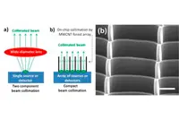 A team of researchers from the University of Surrey’s Advanced Technology Institute (ATI) has grown vertically aligned carbon nanotubes (CNTs), in a grid-like formation on glass. The CNTs create wafer-thin, flat structures that could enable the miniaturisation of a range of optical devices. Removing the need for traditional curved refracting lensing systems, which can be bulky and expensive, will enable new compact optical systems based on this nanotechnology.
The material is either highly transparent or opaque depending on its angle with respect to the beam. This property makes it ideal for either collimating a beam of visible white light; or for absorbing stray light that is off the axis of the CNTs. This is said to enable significant improvement to line-of-sight applications such as optical data transfer, or the rejection of stray light in high specification space telescopes.
James Clark from the ATI explained: “One approach to realising compact optical systems, which is an alternative to that used here, is a Veselago lens which is made from artificial ‘metamaterials’. However, currently the obstacles in translating this theory to practical use are numerous.”
Professor Ravi Silva, director of the ATI, added: “Collimation maintains an accurate record of the image and is classically done by using two lenses, each with a specific shape and placed a certain distance from each other. What we have shown in this study is that carbon nanotubes grown in this way can produce a well-collimated beam of visible light using a single flat material, a practical feature of a Veselago lens. This will lead to a new approach to small and flexible optical devices.”
The next step for this work is to incorporate this material into existing technology. The ATI has already demonstrated low-temperature growth processes to enable direct wafer-scale integration of vertical CNTs with CMOS devices.
Author
Tom Austin-Morgan
Source: www.newelectronics.co.uk