Electronics News
Archive : 11 January 2016 год
 Researchers at the Harvard John A. Paulson School of Engineering and Applied Sciences and the Innovation Centre Iceland have built a polarimeter on a microchip, revolutionising the design of this widely used scientific tool.
When light is reflected or scattered off an object, its polarisation changes and measuring that change reveals a lot of information. In telecommunications, polarisation is used to carry information through fibre optic cables. From medical diagnostics to high-tech manufacturing to the food industry, measuring polarisation reveals critical data.
Scientists rely on polarimeters to make these measurements. While ubiquitous, many polarimeters currently in use are slow, bulky and expensive. Chip-based polarimeters could provide comprehensive and real-time polarisation monitoring, which could boost network performance and security and help providers keep up with the rising demand for bandwidth.
Federico Capasso, Professor of applied physics at Harvard, said. "Having a microchip polarimeter will make polarisation measurements available for the first time to a much broader range of applications, including in energy-efficient, portable devices."
J. P. Balthasar Mueller, a graduate student in Capasso’s lab, added: "Taking advantage of integrated circuit technology and nanophotonics, the new device promises high-performance polarisation measurements at a fraction of the cost and size."
Capasso's team was able to reduce the complexity and size of polarimeters by building a two-dimensional metasurface covered with an array of metallic antennas, smaller than a wavelength of light, embedded in a polymer film. As light propagates down an optical fibre and illuminates the array, a small amount scatters in four directions. Four detectors measure the intensity of the scattered light and combine to give the state of polarisation in real time.
"One advantage of this technique is that the polarisation measurement leaves the signal mostly intact," added Mueller. "This is crucial for many uses of polarimeters, especially in optical telecommunications, where measurements must be made without disturbing the data stream."
In telecommunications, optical signals propagating through fibres will change their polarisation in random ways. New integrated photonic chips in fibre optic cables are sensitive to polarisation, and if light reaches a chip with the wrong polarisation, it can cause a loss of signal.
"The design of the antenna array makes it robust and insensitive to the inaccuracies in the fabrication process, which is ideal for large scale manufacturing," said Kristjan Leosson, senior researcher and division manager at the Innovation Centre.
Leosson's team in Iceland is currently working on incorporating the metasurface design from the Capasso group into a prototype polarimeter instrument.
Author
Tom Austin-Morgan
Source: www.newelectronics.co.uk
 The manufacture of high performance low power electronics devices based on graphene nanoribbons is likely to be possible, according to an international research team based at Tohoku University’s Advanced Institute of Materials Research.
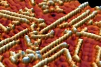
In its work, the team used molecular assemble to connect chiral edge graphene nanoribbons (GNRs) with zigzag edges and demonstrated electronic connection between the GNRs. The team added its work showed the electronic architecture at the interconnection points between two GNRs is the same as that along single GNRs.
“Current molecular assemblies either produce straight GNRs (without identifiable interconnection points) or randomly interconnected GNRs,” said Dr Patrick Han, the project leader. “These growth modes have too many intrinsic unknowns for determining whether electrons travel across graphene interconnection points smoothly. The key is to design a molecular assembly that produces GNRs that are systematically interconnected with clearly distinguishable interconnection points.”
The team grew GNRs on a copper substrate, which confined GNR growth to six directions. It then visualised the structures using scanning tunnelling microscopy (STM). By controlling the precursor molecular coverage, GNRs from different growth directions were connected, producing elbow structures.
“The major finding of this work is that interconnected GNRs do not show electronic disruption,” said Dr Han. “These results show that finding a way to connect defect free GNRs to desired electrodes may be the key strategy toward achieving high performance, low power consumption electronics.”
Author
Graham Pitcher
Source: www.newelectronics.co.uk

