
Electronics News
Archive : 14 February 2016 год
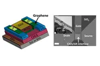 A group of scientists from at the US Department of Energy's (DOE) Brookhaven National Laboratory, Stony Brook University (SBU), and the Colleges of Nanoscale Science and Engineering at SUNY Polytechnic Institute claim to have developed a method for creating resilient, customised, and high-performing graphene: layering it on top of common glass. This scalable and inexpensive process is hoped to help pave the way for a new class of microelectronic and optoelectronic devices, from solar cells to touch screens.
The team initially set out to optimise a solar cell containing graphene stacked on a high-performance copper indium gallium diselenide (CIGS) semiconductor, which in turn was stacked on an industrial soda-lime glass substrate.
Nanditha Dissanayake, formerly of Brookhaven Lab, said: "The sodium inside the soda-lime glass creates high electron density in the graphene, which is essential to many processes and has been challenging to achieve."
The scientists then conducted preliminary tests to provide a baseline for the effects of subsequent doping. But these tests showed that the graphene was already optimally doped without the introduction of any additional chemicals.
"To our surprise, the graphene and CIGS layers already formed a good solar cell junction," Dissanayake said. "After much investigation, and the later isolation of graphene on the glass, we discovered that the sodium in the substrate automatically created high electron density within our multi-layered graphene."
The scientists are now going to probe more deeply into the fundamentals of the doping mechanism and more carefully study the material's resilience during exposure to real-world operating conditions.
Matthew Eisaman, a physicist at Brookhaven Lab and professor at SBU, said: "Now that we have demonstrated the basic concept, we want to focus next on demonstrating fine control over the doping strength and spatial patterning."
They say that initial results suggest the glass-graphene method is much more resistant to degradation than many other doping techniques.
Graphene's high conductivity and transparency make it a promising candidate as a transparent, conductive electrode to replace the relatively brittle and expensive indium tin oxide (ITO) in applications such as solar cells, OLEDs, flat panel displays, and touch screens. In order to replace ITO, scalable and low-cost methods must be developed to control graphene's resistance to the flow of electrical current by controlling the doping strength.
"The potential applications for graphene touch many parts of everyone's daily life, from consumer electronics to energy technologies," Eisaman explained. "It's too early to tell exactly what impact our results will have, but this is an important step toward possibly making some of these applications truly affordable and scalable."
Author
Tom Austin-Morgan
Source: www.newelectronics.co.uk
![]() Researchers from the Optical Networks Group at University College London (UCL) claim to have set a record for the fastest ever data rate for digital information. The group achieved a rate of 1.125Tbit/s as part of research on the capacity limits of optical transmission systems, designed to address the growing demand for fast data rates.
Researchers from the Optical Networks Group at University College London (UCL) claim to have set a record for the fastest ever data rate for digital information. The group achieved a rate of 1.125Tbit/s as part of research on the capacity limits of optical transmission systems, designed to address the growing demand for fast data rates.
Lead researcher, Dr Robert Maher, UCL Electronic & Electrical Engineering, said: “For comparison this is almost 50,000 times greater than the average speed of a UK broadband connection of 24Mbit/s, which is the current speed defining ‘superfast’ broadband.”
The team determined the best way of encoding information in optical signals, taking into account the limitations of the transmitter and receiver. They then applied coding techniques commonly used in wireless communications, but not yet widely used in optical communications, to ensure the transmitted signals are adapted to distortions in the system electronics.
The researchers custom built an optical communication system with 15 channels, each carrying an optical signal of different wavelength, were modulated using the 256QAM format typically used in cable modems, combined and sent to a single optical receiver for detection. By grouping the channels together, the team created a ‘super-channel’ which although not yet commercially available, is believed to be a way forward for the next generation of high-capacity communication systems.
Dr Maher explained: “Using high-bandwidth super-receivers enables us to receive an entire super-channel in one go. Super-channels are becoming increasingly important for core optical communications systems, which transfer bulk data flows between large cities, countries or even continents.”
He added: “However, using a single receiver varies the levels of performance of each optical sub-channel so we had to finely optimise both the modulation format and code rate for each optical channel individually to maximise the net information data rate. This ultimately resulted in us achieving the greatest information rate ever recorded using a single receiver.”
In this study, the researchers connected the transmitter directly to the receiver to achieve the maximum data rate. They will now test the system and measure the achievable data rates in a long distance transmission scenario where optical signals can become distorted as they travel through thousands of kilometres of optical fibres.
Author
Tom Austin-Morgan
Source: www.newelectronics.co.uk
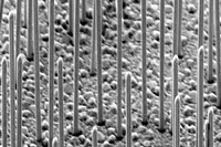 Physicists at the Technical University of Munich (TUM) claim to have developed a nanowire lasers grown on a silicon chip, making it possible to produce high-performance photonic components cost-effectively. The scientists say that this will pave the way for fast and efficient data processing with light in the future.
The miniaturisation of electronics is now reaching its physical limits. "Today already, transistors are merely a few nanometers in size. Further reductions are horrendously expensive," said Professor Jonathan Finley, director of the Walter Schottky Institute at TUM. "Improving performance is achievable only by replacing electrons with photons."
The first silicon-based photonics chips already exist. However, the sources of light for the transmission of data must be attached to the silicon in complicated manufacturing processes. However, Dr Gregor Koblmüller and his team at the Department of Semiconductor Quantum-Nanosystems has, in collaboration with Prof Finley, developed a process to deposit nanolasers directly onto silicon chips.
Growing a III-V semiconductor onto silicon requires experimentation. "The two materials have different lattice parameters and different coefficients of thermal expansion. This leads to strain," explains Koblmüller. "For example, conventional planar growth of gallium arsenide (GaAs) onto a silicon surface results therefore in a large number of defects."
By depositing nanowires that are freestanding with a footprint of a few square nanometers, the scientists could preclude the emergence of defects in the GaAs material.
Team member, Benedikt Mayer, explained: "The interface between gallium arsenide and silicon does not reflect light sufficiently. We thus built in an additional mirror - a 200nm thick silicon oxide layer that we evaporated onto the silicon. Tiny holes can then be etched into the mirror layer. Using epitaxy, the semiconductor nanowires can then be grown atom for atom out of these holes."
The wires can then be grown laterally once they protrude beyond the mirror surface - until the semiconductor is thick enough to allow photons to move back and forth to allow stimulated emission and lasing. "This process is very elegant because it allows us to position the nanowire lasers directly onto waveguides in the silicon chip," said Koblmüller.
Currently, the gallium arsenide nanowire lasers produce infrared light at a predefined wavelength and under pulsed excitation. "In the future we want to modify the emission wavelength and other laser parameters to better control temperature stability and light propagation under continuous excitation within the silicon chips," added Finley.
The team now wants to create an electric interface so that the nanowires operate under electrical injection instead of relying on external lasers.
Pic: Gallium-arsenide nanowires on a silicon surface.
Author
Tom Austin-Morgan
Source: www.newelectronics.co.uk
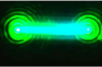 Researchers at Berkeley Labs in the US say that nanowires with diameters as small as 200nm can be tuned to a range of light including visible green and blue wavelengths. The team believes the breakthrough, which supports the emission of bright and stable laser light is ‘promising’ for optoelectronics. Nanoscale lasers could bring optical communications to handheld devices
The researchers used a self assembling blend of caesium, bromine and lead to create the nanowires and pointed out the same blend has proven effective in high efficiency solar cells. “What’s amazing is the simplicity of the chemistry,” said Peidong Yang, a chemist in Berkeley Labs’ Materials “There has been so much progress with these materials in just the past several years and I have a feeling these materials will open a new research frontier for optoelectronics.”
Selected nanowires were placed on a quartz base and excited by another laser, causing them to emit light. Researchers found the nanowire lasers emitted light for more than 1billion cycles after being hit by an ultrafast pulse of visible violet light.
The team says there are opportunities to test other materials and learn whether they improve performance, including substituting tin for lead.
Author
Graham Pitcher
Source: www.newelectronics.co.uk