 Researchers from the Naval Research Laboratory (NRL) in Washington, DC have demonstrated that a combination of two technologies – one to create a thin film and the second to ‘cut’ designs from the film – could be a way to create custom electronic components.
The approach combines the attributes of laser induced forward transfer, or LIFT, with polymer assisted deposition (PAD). In LIFT, a laser beam vaporises a thin layer of solvent and ejects the ink or paste from the film. PAD works by dissolving metal salts in a solution containing polymers and spreading this in a thin layer, which is then heat cured to decompose the polymer.
The NRL team is working with inks containing vanadium dioxide (VO2), which undergoes a ‘sharp’ semiconductor to metal phase transition near room temperature. This, says the team, makes it suitable for applications such as chemical sensors, electrical and optical switches and coatings that change colour with temperature.
“There has not been much overlap between groups that study PAD and those that study LIFT,” said NRL fellow Eric Breckenfeld. “We are one of the first groups to try combining the two techniques.”
Breckenfeld and his colleagues explored a variety of solvents and heating steps to optimise the growth of VO2 films on glass and crystalline substrates, then experimented using LIFT to print patterns with the PAD solutions.
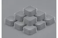
So far, the team has successfully printed simple patterns. Breckenfeld said the results show that LIFT and PAD technologies combined could directly print a range of commercially attractive electronic materials.
Pic: Eric Breckenfeld/NRL
Author
Graham Pitcher
Source: www.newelectronics.co.uk

