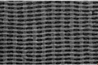
 An MIT research team has described a first technique for stacking layers of block copolymer wires in such a way that the wires in one layer orient themselves perpendicularly to those in the layer below. According to the team, this ability to produce ‘mesh structures’ could make self assembly a more practical way to manufacture memories and optical chips, as well as future processors.
The constituents of a block copolymer are chosen for their chemically incompatibility and their attempts to push away from each other causes them to self organize.
The MIT researchers selected one carbon based and one silicon based polymer. In their efforts to escape the carbon based polymer, the silicon-based polymers fold in on themselves, forming cylinders with loops of silicon-based polymer on the inside. When the cylinders are exposed to an oxygen plasma, the carbon based polymer burns away, while the silicon oxidises to leave glass-like cylinders attached to a base.
A second layer of cylinders can be created by repeating the process, using copolymers with slightly different chain lengths. The cylinders in the new layer naturally orient themselves perpendicularly to those in the first.
If the surface on which the first group of cylinders is formed is treated chemically, the cylinders will line up in parallel rows. The second layer of cylinders will then form parallel rows, perpendicular to those in the first.
But if the bottom layer of cylinders forms haphazardly, the cylinders in the second layer will maintain their relative orientation, creating their own elaborate, but perpendicular, patterns.
While the glass-like wires are said not to be directly useful for electronic applications, the team thinks it might be possible to seed them with other molecules, which would make them electronically active, or to use them as a template for depositing other materials.
Patrick Theofanis, an Intel engineer, said: “In general, the ability to pattern square holes is very useful. If you think of the back end of our chips, we have the back end wiring and then the interconnect layers between those back-end metal layers; that’s where you’d like to be able to punch through holes and connect one layer to the next one. It’s an attractive technology because the aspect ratio is very tunable.”
Author
Graham Pitcher
Source: www.newelectronics.co.uk

