
 The Centre for Process Innovation (CPI) and Heidelberg Instruments have developed a high resolution, high speed roll to roll digital lithography tool for the manufacture of flexible organic thin film transistors (OTFT) used in next generation applications such as foldable display screens, sensors, integrated circuits and photo-detectors.
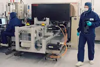
The machine, installed at CPI’s National Printable Electronics Facility in County Durham, is described as a stepping stone in the commercialisation of printable electronic devices as it provides the ability to continuously manufacture OTFTs directly onto rolls of plastic film at rates approaching 0.1m2/minute.
Products that use thin-film transistors with non-standard shapes and sizes or custom integrated circuits struggle to reach mass market adoption due to the high cost of manufacturing smaller volumes and the limitations imposed by print resolution and production speed. Digital lithography, sometimes referred to as ‘laser direct imaging’ or LDI, eliminates the need for photomasks by guiding a laser with computer generated imagery to directly expose light-sensitive material. This reduces production time and lowers manufacturing cost, opening the technology up for shorter production runs and custom designs.
Roland Kaplan, R&D manger at Heidelberg Instruments, said: “We developed the write engine for this roll to roll lithography tool based on our experiences in high resolution optics, UV Laser and DMD technology. The main aspects were the modularity of the optical engine, the flexibility of the interfaces to the control system and the capability to handle the high speed data volume.”
The key feature of the new tool is its ability to expose rolls of film with digital images generated in real time, allowing it to compensate for any distortions present in each layer of the transistor as it is built up. It does this by using a state-of-the-art optical exposure engine along with a laser and digital mirror device capable of through-putting up to 150Mbytes/s of image data. The system is capable of 4µm line and space resolution in the printed pattern using a print density equivalent to 25,000 dots per inch. It uses an exposure wavelength of 355nm and is compatible with a range of standard i-line photoresist materials as well as being suitable for other UV-curing processes.
Dr Tom Harvey, business development manager at CPI added: “The new tool is available on an open access basis, allowing companies to progress their current sheet processes towards roll to roll production, enabling significant reductions in the costs and times associated with new product development of flexible OTFT arrays.”
The digital lithography line is expected to be of interest to companies who require high resolution continuous patterning of thin films on plastic.
Author
Tom Austin-Morgan
Source: www.newelectronics.co.uk