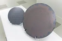
 CEA-Leti claims to have manufactured micro-accelerometers on 300mm wafers, a development that could lead to lower MEMS manufacturing costs.
“This demonstration that our 200mm MEMS platform is now compatible with 300mm wafer fabrication shows a significant opportunity to cut MEMS production costs,” said Leti CEO Marie Semeria. “This will be especially important with the worldwide expansion of the IoT and continued growing demand for MEMS in mobile devices.”
Leti’s M&NEMS technology platform is based on detection by piezo-resistive silicon nanowires, which reduce sensor size and improve performances of multi-axis sensors. Its inertial-sensor manufacturing concept enables the design and fabrication of combo sensors, such as three-axis accelerometers, three-axis gyroscopes and three-axis magnetometers on the same chip;a key component for IoT applications.
Leti’s M&NEMS concept, developed with 200mm technology, is currently being transferred to an industrial partner. Demonstration of this technology on 300mm wafers is said to have shown very promising results.
In addition to lowering costs, manufacturing MEMS with 300mm technology enables 3D integration using MEMS CMOS processes in more advanced nodes than on 200mm, and the use of 3D through-silicon-vias, which is already available in 300mm technology.
Pic: 200mm and 300mm M&NEMS wafers
Author
Tom Austin-Morgan
Source: www.newelectronics.co.uk

