
 National Institute of Standards and Technology (NIST) researchers claim to have used optical microscopes emitting tiny fractions of the wavelength of light to measure chip features that are approaching 10nm.
Using a microscope that combines standard through-the-lens viewing with a technique called scatterfield imaging, the NIST team accurately measured patterned features on a silicon wafer that were 30 times smaller than the wavelength of light (450nm) used to examine them. They reported that measurements of the 16nm etched lines on a wafer were accurate to 1nm. With the technique, they spotted variations in feature dimensions amounting to differences of a few atoms.
The team’s measurements were confirmed by those made with an atomic force microscope, which achieves sub-nanometre resolution but is considered too slow for online quality-control measurements.
Richard Silver, the physicist who initiated NIST's scatterfield imaging effort, said: "Light-based, or optical, microscopes can't ‘see’ features smaller than the wavelength of light, at least not in the crisp detail necessary for making accurate measurements. However, light does scatter when it strikes so-called subwavelength features and patterned arrangements of such features.
“Historically, we would ignore this scattered light because it did not yield sufficient resolution. Now we know it contains helpful information that provides signatures telling us something about where the light came from,” he continued.
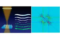
With scatterfield imaging, Silver and colleagues methodically illuminated a sample with polarised light from different angles. From this collection of scattered light the NIST team can extract characteristics of the bounced lightwaves that reveal the geometry of features on the specimen.
"It's the ensemble of data that tells us what we're after," says project leader Bryan Barnes." We may not be able see the lines on the wafer, but we can tell you what you need to know about them - their size, their shape, their spacing."
The NIST researchers can use standard equations to simulate light scattering from an ideal, defect-free pattern. Using wave analysis software they developed, the team has assembled a library of light-scattering reference models. So once a specimen is scanned, the team relies on the program to compare their real-world data to models and to find close matches.
The next steps for the researchers include extending the technique to even shorter wavelengths of light, down to ultraviolet, or 193nm to accurately measure features as small as 5nm.
Pic: Illustration of how tiny changes in wavy images scattered from lines in a grid-like array can be reconstructed when paired with advanced optical and computational techniques. Coloring corresponds to the magnitude of the variance for specific data points
Author
Tom Austin-Morgan
Source: www.newelectronics.co.uk