
 A team of researchers from the US Department of Energy’s Oak Ridge National Laboratory (ORNL) have developed a processing technique that could bring two-dimensional electronic devices closer to their ultimate promise of low power, high efficiency and mechanical flexibility.
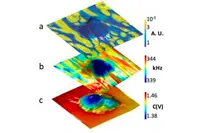
Led by Olga Ovchinnikova of ORNL's Centre for Nanophase Materials Sciences Division, the team used a helium ion microscope on a layered ferroelectric surface of a bulk copper indium thiophosphate. This resulted in the discovery of a material with tailored properties potentially useful for mobile phones, photovoltaics, flexible electronics and screens.
Ovchinnikova said: "Our method opens pathways to direct-write and edit circuitry on 2D material without the complicated current state-of-the-art multi-step lithographic processes."
The team noted that while the helium ion microscope is typically used to cut and shape matter, they demonstrated that it can also be used to control ferroelectric domain distribution, enhance conductivity and grow nanostructures. Their work could establish a path to replace silicon as the choice for semiconductors in some applications.
Alex Belianinov, part of Ovchinnikova’s team, said: "Everyone is looking for the next material - the thing that will replace silicon for transistors. 2D devices stand out as having low power consumption and being easier and less expensive to fabricate without requiring harsh chemicals that are potentially harmful to the environment."
Pic: This diagram illustrates the effect of helium ions on the mechanical and electrical properties of the layered ferroelectric
Author
Tom Austin-Morgan
Source: www.newelectronics.co.uk