
 The basis for growing wafer-scale two-dimensional crystals for future electronic devices has been published in two online nanotechnology journals.
Growing high-quality, crystalline 2D materials at scale has proven to be a challenge, but a team of researchers, led by Professor Joan Redwing of the National Science Foundation and Penn State, claim to have developed a multistep process to make single crystal, atomically thin films of tungsten diselenide across large-area sapphire substrates.
"Up until now, the majority of 2D devices have been fabricated using small flakes that are exfoliated off of bulk crystals," Prof Redwing said. "To develop a device-ready technology, you have to be able to make devices on large-area substrates and they have to have good crystal quality."
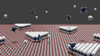
The process uses sapphire as the substrate because of its crystalline structure. This structure orients the film growth in a crystal pattern through epitaxy.
As small islands of the material form on the substrate and the substrate is heated, the islands spread out across the substrate in a uniform pattern. This is said to form a large-area film without gaps and with few defects.
According to the team, the key was the use of gas-source chemical vapor deposition, which they used to control the island density and the rate of spreading to achieve a single layer of the 2D material.
A team led by associate professor Joshua Robinson of Penn State is said to have now provided the foundational understanding to enable device-ready synthetic 2D semiconductors based on these epitaxial large-area films in future industrial-scale electronics.
"The primary significance of this work is we were able to achieve an understanding of the extrinsic factors that go into having a high-quality 2D material," Robinson explained. "What we found was that even when you grow oriented crystals on a surface, there are other factors that impact the ability to get high electron mobility or fast transistors."
The team said that they discovered a strong interaction between the sapphire substrate and the monolayer film, with the substrate dominating the properties. To overcome these challenges, they grew two or three layers which they said improved the performance by factors of up to 100 times.
"This is the first real evidence of the effect of the substrate on the transport properties of 2D layers," Robinson concluded.
Author
Bethan Grylls
Source: www.newelectronics.co.uk