
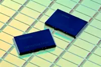
 Toshiba has announced a method of embedding flash memory based on 65nm logic process that uses less power than current mainstream technology, and a single-poly non-volatile memory (NVM) process based on 130nm logic and analogue power. Applying the optimal process to various applications will allow Toshiba to expand its product line-up in such areas as microcontrollers, wireless communication ICs, motor controller drivers and power supply ICs.
There is demand in the IoT market for low power consumption in areas including wearable and healthcare-related equipment. Toshiba has adopted Silicon Storage Technology's third-generation SuperFlash cell, in combination with its own 65nm logic process technology. Microcontrollers for consumer and industrial applications that apply the process are said to consume 60% less power than that of current mainstream technology.
Following the first series of microcontrollers, Toshiba plans to release sample Bluetooth Low Energy products, as well as apply the 65nm process to its wireless communication IC product family that can optimise use of low power consumption characteristics, including contactless cards.
As well as developing products for IoT, the company also aims to lower power consumption for entire systems, targeting 50µA/MHz operation. In applications where significant cost reductions are a concern, Toshiba claims it has developed an NVM embedded process that adopts Yield Microelectronics Corporation's single-poly multi-time programmable cells on Toshiba's 130nm logic process technology. This is said to improve performance while limiting increased steps in mask pattern lithography to three or fewer.
Author
Tom Austin-Morgan
Source: www.newelectronics.co.uk