
 Physicists at the Technical University of Munich (TUM) claim to have developed a nanowire lasers grown on a silicon chip, making it possible to produce high-performance photonic components cost-effectively. The scientists say that this will pave the way for fast and efficient data processing with light in the future.
The miniaturisation of electronics is now reaching its physical limits. "Today already, transistors are merely a few nanometers in size. Further reductions are horrendously expensive," said Professor Jonathan Finley, director of the Walter Schottky Institute at TUM. "Improving performance is achievable only by replacing electrons with photons."
The first silicon-based photonics chips already exist. However, the sources of light for the transmission of data must be attached to the silicon in complicated manufacturing processes. However, Dr Gregor Koblmüller and his team at the Department of Semiconductor Quantum-Nanosystems has, in collaboration with Prof Finley, developed a process to deposit nanolasers directly onto silicon chips.
Growing a III-V semiconductor onto silicon requires experimentation. "The two materials have different lattice parameters and different coefficients of thermal expansion. This leads to strain," explains Koblmüller. "For example, conventional planar growth of gallium arsenide (GaAs) onto a silicon surface results therefore in a large number of defects."
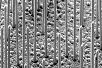
By depositing nanowires that are freestanding with a footprint of a few square nanometers, the scientists could preclude the emergence of defects in the GaAs material.
Team member, Benedikt Mayer, explained: "The interface between gallium arsenide and silicon does not reflect light sufficiently. We thus built in an additional mirror - a 200nm thick silicon oxide layer that we evaporated onto the silicon. Tiny holes can then be etched into the mirror layer. Using epitaxy, the semiconductor nanowires can then be grown atom for atom out of these holes."
The wires can then be grown laterally once they protrude beyond the mirror surface - until the semiconductor is thick enough to allow photons to move back and forth to allow stimulated emission and lasing. "This process is very elegant because it allows us to position the nanowire lasers directly onto waveguides in the silicon chip," said Koblmüller.
Currently, the gallium arsenide nanowire lasers produce infrared light at a predefined wavelength and under pulsed excitation. "In the future we want to modify the emission wavelength and other laser parameters to better control temperature stability and light propagation under continuous excitation within the silicon chips," added Finley.
The team now wants to create an electric interface so that the nanowires operate under electrical injection instead of relying on external lasers.
Pic: Gallium-arsenide nanowires on a silicon surface.
Author
Tom Austin-Morgan
Source: www.newelectronics.co.uk