This low-cost detector probe allows you to measure RF signals from below 100kHz up to over 1GHz with your DMM for signal voltages between about 20mV and 10 V RMS. You can use it with a probe or a sniffer loop and you can even use it to measure the voltage across a coaxial cable load and calculate the RF power.
T’S NOT DIFFICULT to measure RF signals if you have access to an RF power meter or spectrum analyser -but these are expensive instruments (£1000 plus). You simply can’t justify their cost, unless you work a lot with RF and communications equipment. So what can you use to make the occasional RF signal measurement?
The usual approach is to use a passive RF detector probe connected to your DMM. By using a Schottky diode in the detector, these can give acceptable results for signals between about 500mV and 50V RMS, and between say 10MHz and 500MHz or so. But they’re usually not much use for measuring signals below 500mV, due to non-linearity of the detector diode’s forward conduction characteristic. Signals larger than about 50 V also tend to be a problem, because of the diode’s maximum reverse voltage rating.
Recently, I needed an RF detector probe that would be capable of measuring quite small signals - much lower than 500mV. I searched on the Internet and found the circuit of an ‘active’ RF detector probe using a nifty linearity compensation scheme developed originally by US radio amateur John Grebenkemper, KI6WX, for use in SWR bridges. This probe was claimed to be useful for measuring signals between 100kHz and 30MHz.
Experimenting with this circuit, I soon realised that its basic configuration could be refined to produce version capable of working up to much higher frequencies. The result is the new design described in this article. It is capable of making measurements from below 100kHz to above 1GHz, for signals from about 20mV up to 10V RMS (in two ranges). It’s low in cost, easy to build and particularly flexible in terms of the measurements it can make.
Circuit details
Fig.1 shows the complete circuit details for the probe. The actual RF detector diode is D1, a very tiny 1PS70SB82 UHF Schottky diode. It’s connected in a standard half-wave configuration and produces a DC voltage across the 10nF filter capacitor that’s very close to the peak value of the RF input signal.
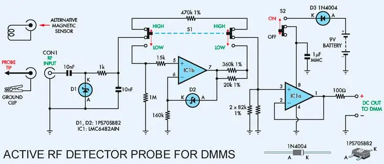
Fig.1: the circuit for the Active RF Detector Probe. When S1 selects the high range, the detected RF signal is rectified by D1, attenuated by a voltage divider and fed to voltage follower stage IC1a, which then drives a DMM. Alternatively, on the low range, the detected signal from D1 is fed to IC1a via a linearity compensation circuit based on op amp IC1b.
When range switch S1 is in the HIGH position, this DC voltage is fed to the pin 3 input of op amp IC1a via a resistive voltage divider formed by a 470ΩQ resistor and two paralleled 82ΩQ resistors. The divider ratio is set so that the DC voltage fed to pin 3 of IC1a is equal to 0.0707 times the peak value of the input voltage, after allowing for losses in the detector, corresponding to one-tenth of the RMS value of the RF input.
Since IC1a (one half of an LMC6482 dual CMOS op amp) is connected as a voltage follower, this is the voltage fed out to the DMM.
Why do we attenuate the detector output by 0.0707 on this range and not just by 0.707, corresponding to the full RMS voltage of the RF input? It’s because IC1 is operating from a supply voltage of about 8.4V (9V minus the 0.6V drop in D3), and so it can’t handle signal levels greater than this. By dividing down by 10 as well, we allow the probe to measure signals up to the PIV (peak inverse voltage) rating of D1. This is 15 V, corresponding to an RF input of 10.6V RMS.
So when the probe is switched to the HIGH range, the output of the detector diode is fed without any linearity compensation to IC1a, via the voltage divider. IC1a feeds this uncompensated DC voltage out to the DMM, merely lowering the source impedance so that accurate readings should be produced regardless of the DMM’s input resistance. In any case most DMMs have an input resistance of 10MΩ or more on the DC voltage ranges.
On the HIGH range, the probe can measure RF signals between about 600mV and 10V RMS. The only complication on this range is that there’s a built-in 10:1 division, so the DMM reads one-tenth the RMS value of the RF input signals, ie, 1.00V RMS becomes 100mV DC and so on.
Low range
Things get a little more interesting when you move range switch S1 to the LOW position. As you can see, this switches the 470kΩ divider resistor out of circuit and instead switches in a ‘linearity compensation’ circuit based on IClb and diode D2, another 1PS70SB82 Schottky diode.
IC1b is connected as a non-inverting amplifier stage, with D2 forming part of the negative feedback circuit - along with a 160kΩ resistor connected from pin 6 to ground. The combination of D2 and the 160kΩ resistor forms a nonlinear voltage divider. This divider varies IC1b’s gain according to the DC voltage level at its pin 7 output, in a manner that closely compensates for the non-linearity in detector diode D1.
As a result, the DC voltage at pin 7 is closely proportional to the peak level of the probe’s RF input voltage, at levels right down to 20mV.
The paralleled 360kΩ and 20kΩ resistors connected from pin 7 of IC1b to the LOW side contact of switch S1 form the upper leg of an output voltage divider for this range, with the lower leg formed by the two paralleled 82kΩ resistors from pin 3 of IC1a to ground. The division ratio of this divider is arranged to make the DC voltage appearing at pin 3 of IC1a directly proportional to the RMS value of the RF input voltage, so that for this range the DMM reads the amplitude of the RF input signals directly.
Power for IC1 comes from a standard 9V alkaline battery, with diode D3 connected in series for reverse polarity protection. As the current drawn by IC1 is typically less than 2mA, the battery should last for almost its shelf life with intermittent use. And that’s all there is to the circuit operation.
Linearity performance
The performance you can expect from the Active RF Detector Probe can be seen in the linearity plots of Fig.2 and the frequency response plot of Fig.3. The upper plot (A) in Fig.2 shows the linearity at the lower end of the HIGH range and as you can see, it moves away from the linear reference line (red) at levels below 600mV.
By contrast, the lower plot (B) in Fig.2 shows the linearity at the low end of the LOW range. Here you can see that the DC output only deviates from the red linear reference line at RF levels below 20mV.
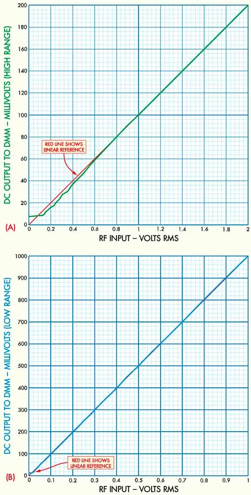
Fig.2: the top graph (A) shows how the linearity response (green) on the HIGH range deviates from the linear reference line (red) for signal levels below 600mV. By contrast, the bottom graph (B) shows that the linearity response on the LOW range only deviates from the red reference line for levels below 20mV due to the response of the linearity compensation circuit.
Fig.3 shows the measured frequency response of our prototype RF Detector Probe. It’s quite flat, at about ±5% up to about 200MHz, then rises up to a peak at 500MHz and to an even larger peak at 750MHz. These peaks are presumably due to resonances in the probe’s input circuit (involving D1, the 10nF input coupling capacitor and input connector CON1) and would probably be very hard to remove.
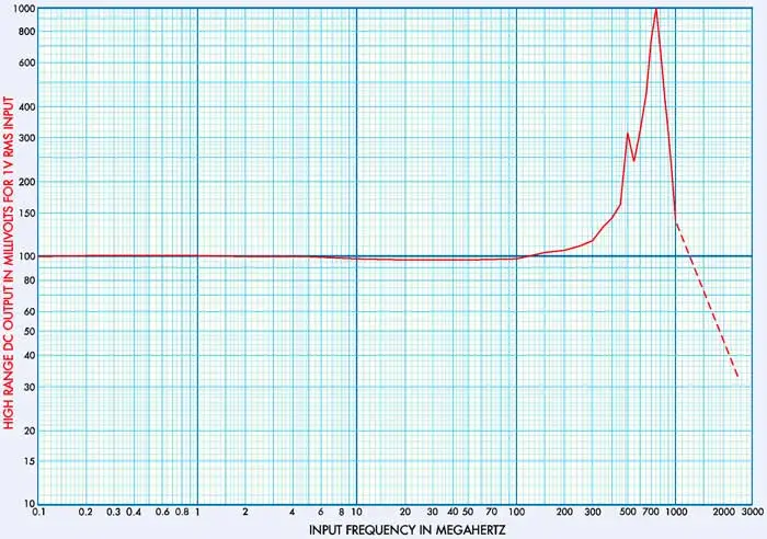
Fig.3: the frequency response of the prototype Active RF Detector Probe. It’s quite flat up to about 200MHz but then rises steeply to peaks at 500MHz and 750MHz. Use this graph and the plots in Fig.2 to correct the measured RF voltage reading if necessary.
D1, the 10nF capacitors and the 1kΩ resistor are all SMD components and D1 and the 10nF input capacitor are positioned on the PCB as close as possible to CON1. This also helps to ensure good linearity up to 200MHz.
By the way, although the peaks at 500MHz and 750MHz look quite dramatic, they don’t mean that the Active RF Detector Probe can only be used to make measurements below 200MHz. On the contrary, Fig.3 can be used as a correction curve when making measurements up to 1GHz (1000MHz).
One last point about Fig.3. You might wonder about the significance of the dashed red line extending the plot from 1GHz to 2.45GHz. It’s simply my ‘best guess’ of the probe’s response above 1GHz, based on some measurements I was able to make at 2.414GHz, 2.432GHz and 2.450GHz using a small UHF generator module. My main RF signal generator only functions up to 1000MHz, so I couldn’t make any measurements between 1.00GHz and 2.414GHz. That’s why the response line is dashed over this section.
Parts List | |
1 ABS instrument case, 120 х 60 х 30mm 1 double-sided PCB, available from the EPE PCB Service, code 04107131, 61 х 29mm 2 PCB-mount subminiature DPDT slide switches 2 M3 х 20mm machine screws 2 M3 х 6mm machine screws 2 M3 х 9mm untapped spacers 2 M3 х 10mm untapped nylon spacers (5mm OD) 4 M3 hex nuts 2 M3 flat washers 2 M3 lockwashers 2 40 x 8mm strips of 0.25mm sheet brass 1 panel-mount BNC socket (CON1) 2 crimp-type BNC line plugs, RG6 cable type 1 plastic cable gland (3-6mm cable size) 2 banana plugs, 1 red, 1 black 1 9V battery snap 1 9V alkaline battery 1 black alligator clip lead | 1 1.5m length of light-duty 2-core red/black cable 1 30mm length of 1mm-diameter hard brass wire 1 100mm length of 1mm-diameter enamelled copper wire 1 35mm length 6mm- dia heatshrink tubing Semiconductors 1 LMC6482AIN dual CMOS op amp (IC1) 2 1PS70SB82 UHF Schottky diodes (D1,D2) 1 1N4004 silicon diode (D3) Capacitors 2 10nF 1206 SMD ceramic 1 1 μF MMC ceramic Resistors (0.25W, 1%) 1 1MΩ 2 82kΩ 1 470kΩ 1 20kΩ 1 360kΩ 1 15kΩ 1 160kΩ 1 1kΩ 0805 SMD 1 100Ω |
Construction
Almost all the parts are mounted on a small double-sided PCB, available from the EPE PCB Service, coded 04107131 and measuring 61 x 29mm. This assembly is housed in a compact ABS instrument case measuring 120 x 60 x 30mm.
The only parts not mounted on the PCB are RF input connector CON1 (which is fitted to an end panel), the cable gland used to anchor the DC output cable (mounted on the other end panel) and the 9V battery which is mounted inside the case behind the PCB.
Virtually all the parts on the PCB are mounted on the top, the exceptions being slide switches S1 and S2. These are mounted on the underside of the board, so that their actuators can later protrude through matching slots in the case lid (see photo).
Follow Fig.4 to install the parts on the PCB. It’s a good idea to fit the five SMD parts first. These parts are all mounted in the upper lefthand area of the PCB, very close to the connections for input socket CON1. The only polarised SMD parts are D1 and D2, which should both be fitted with their ‘two-lead’ sides towards the top of the PCB.
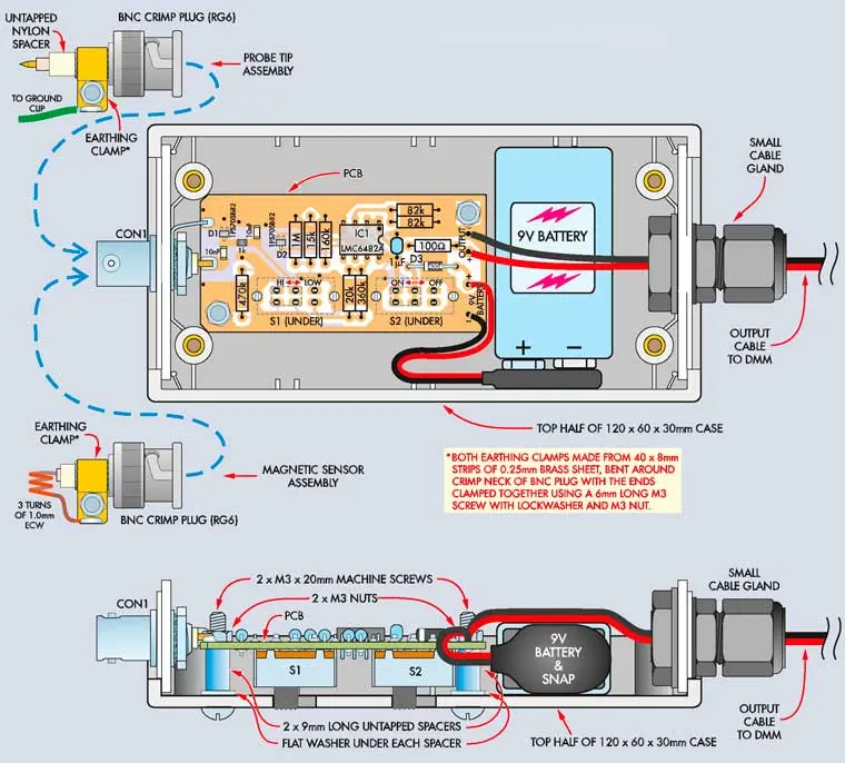
Fig.4: install the parts on the PCB and complete the wiring as shown in this diagram. The two probe assemblies are also shown (see text), along with the mounting details for the PCB inside the plastic instrument case. Note that switches S1 and S2 are installed in the underside of the PCB, so that their actuators protrude through the case lid.
Once the SMDs have been installed, the remaining parts can be added. These include the through-hole resistors, the 1pF MMC capacitor, diode D3, IC1 and finally the two slide switches on the underside. That done, solder the battery snap lead in place.
The next step is to solder a 1.5m length of light-duty red/black figure-8 cable to the PCB output terminals. Make sure that the red wire goes to the OUTPUT+ PCB pad and the black lead to the OUTPUT- pad. Once that’s done, the PCB assembly is complete and ready for mounting in the case.
Preparing the case
The next step is to drill and cut the various holes required in the top half of the case and the two end panels. The locations and sizes for all of these holes are shown in Fig.5. The four circular holes can be drilled and/or reamed to size and in each case, it’s best to start with a small pilot drill.
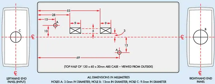
Fig.5: this diagram can either be copied or downloaded from the EPE website and used as a template for drilling the two end panels and the top half of the case. The switch cutouts can be made by drilling a series of small holes around the inside perimeter, then knocking out the centre piece and filing to shape.
The two rectangular holes are for S1 and S2. They can be made by first drilling a series of small holes around the inside perimeter, then knocking out the centre piece and carefully filing them to shape using jeweller’s needle files.
Once all the holes have been made, download the front-panel artwork (in PDF format) from the EPE website, print it out and laminate it. Alternatively, if you don’t have access to a hot laminator, print it out onto photo paper. That done, cut out the switch holes and the two screw holes using a hobby knife, trim the label to size and attach it to the upper half of the case using double-sided tape.
The PCB assembly can now be mounted inside the upper half of the case. Fig.4 shows the mounting details. As can be seen, it’s supported on two M3 x 9mm untapped spacers plus a flat washer under each spacer, and secured using M3 x 20mm machine screws and M3 nuts.
The flat washer under each spacer is necessary to ensure that the PCB is spaced up from the case by nearly 10mm. This allows the slide switches to just protrude through their matching rectangular holes and, at the same time, ensures that the top of the PCB subsequently sits just under the centre contact spigot of CON1.
CON1 can now be mounted on the lefthand end panel. Make sure that its earthing lug is oriented horizontally in the direction shown on Fig.4 and that the attachment nut is firmly tightened. This panel is then lowered into the lefthand end of the case and CONl’s earth lug bent around as shown so that it sits just above the matching earth solder pad on the PCB.
The earth lug and CONl’s centre spigot can now be soldered to their respective pads.
Table 1: Resistor Colour Codes
No. | Value | 4-Band Code (1%) | 5-Band Code (1%) |
1 | 1MΩ | brown black green brown | brown black black yellow brown |
1 | 470kΩ | yellow violet yellow brown | yellow violet black orange brown |
1 | 360kΩ | orange blue yellow brown | orange blue black orange brown |
1 | 160kΩ | brown blue yellow brown | brown blue black orange brown |
2 | 82kΩ | grey red orange brown | grey red black red brown |
1 | 20kΩ | red black orange brown | red black black red brown |
1 | 15kΩ | brown green orange brown | brown green black red brown |
1 | 100Ω | brown black brown brown | brown black black black brown |
Final assembly
Now for the final assembly. First, slip a 35mm-long length of 6mm-diameter heatshrink over the output cable and slide it right down to the PCB (it later runs across the battery). That done, fit the cable gland to the righthand end-panel, then pass the output cable through it and lower this end assembly into place.
The next step is to fit the battery, after which most of the slack can be taken out of the output cable and the cable gland tightened. The battery will now be secured under the output cable, with the heatshrink running across it.
The free-end of the output cable must be fitted with banana plugs, to make the connection to the DMM. Fit a red plug to the red (+) output lead and a black plug to the black (-) lead.
The Active RF Detector Probe assembly is now complete and you can fit the lower half of the case, fastening it all together using the four countersink-head M3 screws supplied with it.
Specifications |
|
Making the probe tips
Before using the unit, you first have to make the two interchangeable probe tips - or to be more accurate, a probe tip and a magnetic sensor (or sniffer) probe.
As shown in Fig.4, these are both based on a standard crimp-type BNC line plug (ie, where the centre conductor of a coaxial cable is soldered to the plug’s centre pin, but the outer shielding braid is connected to a ferrule on the rear of the plug by crimping it inside a thin metal sleeve).
In this case, we’re using plugs designed for crimping onto RG6 cable, as these have a ferrule with an inner diameter of about 5mm.
Here though, we don’t actually crimp the earth connections to the BNC plug ferrules. Instead, the earth connections are soldered to small P-clamps which are then attached to the ferrules using M3 x 6mm machine screws, lockwash-ers and nuts (see photo).
The P-clamps are bent from 40 x 8mm strips of 0.25mm brass sheet, with 3mm holes drilled in the flat ends to accept the M3 screws. Once made, secure them to the BNC plug ferrules as shown.
Probe tip assembly
The probe tip assembly is made using a 30mm length of lmm-diameter hard brass wire, with a sharp point ground or filed at one end. The other end of this wire is then passed into the rear of the plug’s centre pin and secured by soldering the two together (don’t leave a large solder ‘blob’ at the joint though). That done, the pin-and-tip assembly is pushed all the way into the plug (from the ferrule end) until the pin ‘clicks’ into position inside the connector.
Once the tip assembly is in place, you then slip an M3 x 10mm untapped nylon spacer (outer diameter 5mm) into the rear of the ferrule, to act as an insulator/ dielectric. A short length of PVC insulation from a 230V mains lead conductor is then slipped inside the nylon spacer to support the probe tip more securely. Finally, a short earth lead (eg, about 70mm long) fitted with an alligator clip is soldered to the brass P-clamp.
Magnetic sensor probe
The magnetic sensor (sniffer) probe is made in a similar way. However, instead of using a 30mm-length of brass wire for the tip, we instead use a 100mm-length of lmm-diameter enamelled copper wire, with its centre section first bent around a 3.5mm rod or mandrel (eg, a 3.5mm drill bit) to form three neat turns.
Both ends of the wire are then scraped for about 4mm, after which one end is soldered into the rear of the plug’s centre pin. A nylon spacer and an inner PVC sleeve are then fitted inside the plug’s ferrule, after which the pin end of the coil wire is pushed carefully into place until the pin clicks into position inside the BNC connector.
It’s then just a matter of carefully bending the sniffer coil’s free end into position so that it can be soldered to the previously-installed P-clamp.
Using the RF probe
There are no adjustments to make before using the probe. It’s simply a matter of plugging the output cable into the input jacks of your DMM, setting the DMM to an appropriate DC voltage range (eg, 20.0V, 2.00V or 200mV) and then setting the two switches on the probe.
S2 simply switches the power, while S1’s position mainly depends on the likely signal level that’s to be measured. If you’re not sure of this, it would be a good idea to push S1 into the HIGH position, just to be safe. You can then select the LOW position for a more accurate reading if the signal proves to be lower than about 1V RMS.
Note that if you want to measure RF signal voltages, you’ll mainly want to use the probe tip and its ground lead. That’s because the magnetic sensor provides an induced voltage due to RF current in the circuit you’re testing. So the voltage readings don’t mean much, although they do allow you to make comparisons.
Because we have used a BNC coaxial socket as the input for the Active RF Detector Probe, this also allows it to be used for direct RF voltage measurements in coaxial cables. This means that it can be used in conjunction with a 50Ω coaxial load and a look-up table to make low-power RF power measurements, by using the configuration shown in Fig.6.
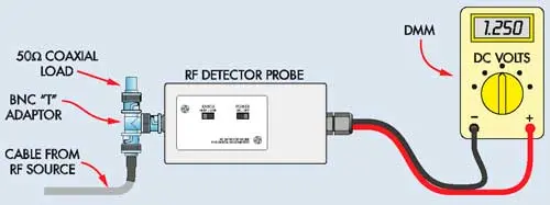
Fig.6: direct RF voltage measurements can be made in coaxial cables by using the configuration shown here. Because the load resistance is known (ie, 50Ω), this also allows you to calculate the RF power (see also Table 2).
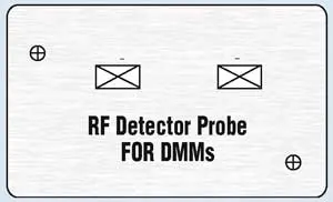
Fig.7: this front-panel artwork can be copied and laminated. The artwork can also be downloaded in PDF format from the EPE website.
Table 2: Volts to Power Conversion
VOLTS rms | POWER (50Ω) | VOLTS rms | POWER (50Ω) |
10.0 | 2.0 W | 446 mV | 4.0 mW |
8.9 | 1.6 W | 398 mV | 3.2 mW |
7.9 | 1.26 W | 354 mV | 2.5 mW |
7.07 | 1.0 W | 316 mV | 2.0 mW |
6.30 | 794 mW | 282 mV | 1.6 mW |
5.62 | 631 mW | 251 mV | 1.26 mW |
5.01 | 501 mW | 224 mV | 1.00 mW |
4.46 | 398 mW | 199 mV | 790 μW |
3.98 | 316 mW | 178 mV | 630 μW |
3.54 | 251 mW | 158 mV | 500 μW |
3.16 | 200 mW | 141 mV | 400 μW |
2.82 | 158 mW | 126 mV | 320 μW |
2.51 | 126 mW | 112 mV | 250 μW |
2.24 | 100 mW | 100 mV | 200 μW |
1.99 | 79 mW | 89 mV | 160 μW |
1.78 | 63 mW | 79 mV | 126 μW |
1.58 | 50 mW | 71 mV | 100 μW |
1.41 | 40 mW | 63 mV | 80 μW |
1.26 | 32 mW | 56 mV | 63 μW |
1.12 | 25 mW | 50 mV | 50 μW |
1.00 | 20 mW | 44.6 mV | 40 μW |
890 mV | 19 mW | 39.8 mV | 32 μW |
790 mV | 12.6 mW | 35.4 mV | 25 μW |
710 mV | 10 mW | 31.6 mV | 20 μW |
630 mV | 8.0 mW | 28.2 mV | 16 μW |
560 mV | 6.3 mW | 25.1 mV | 13 μW |
501 mV | 5.0 mW | 22.4 mV | 10 μW |
As you can see, this involves fitting a BNC T-adaptor to the probe’s input socket and then fitting a 50Ω coaxial load to one side. The input cable from the low-power RF source you want to measure is then connected to the other socket of the T-adaptor, and Bob’s your uncle.
Of course, the Active RF Detector Probe and DMM combination only measures RF voltage; it doesn’t measure power directly. However, it’s relatively easy to convert the voltage level into power, since you also know the load resistance.
For example, if you’re using a 50Ω load as shown in Fig.6, you can use Table 2 to look up the value. Just don’t forget to correct the voltage reading using the plots in Figs.2 and 3 - and also multiply the reading by 10, if you’re using the Probe’s HIGH range - before you convert it to power.
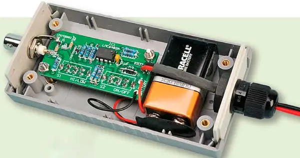
The PCB and the battery are mounted in the top half of the case, which thenn becomes the lid. Although not shown here, we suggest that the battery snap leads be
cable tied to the output cable, to prevent them breaking away at the PCB pads.
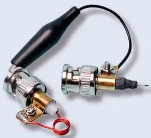
This view shows the two completed RF probes, one using a probe tip and the other a coil to act as a ‘sniffer’.
Author: Jim Rowe

