Sometimes you do not get proper output from a circuit due to faulty ICs. This circuit can test timer 555 and op-amp 741 ICs, which are commonly used in projects, to save you from this problem.
Circuit and working
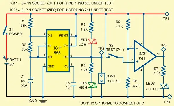
Fig. 1 shows circuit diagram of the tester which is built around the very 555 timer (IC1) and the op-amp 741 (IC2) that are to be tested. IC1 is wired as astable multivibrator with output
frequency of around 1Hz. Resistors R1 and R2 and capacitor C1 are the timing components that decide output frequency. You can change 1Hz frequency by changing values of these components.

Fig. 1: Circuit diagram of 555 and 741 ICs tester
The 555 tester section is basically an LED flasher circuit. Square-wave output at pin 3 of IC1 drives LED1 and LED2 which glow alternately. That is, when pin 3 is low, LED1 glows and when pin 3 is high, LED2 glows. This indicates that the 555 timer under test is in good condition. If the 555 is faulty, both the LEDs mayremain off or glow dimly, or one or both of them may glow continuously. Between pin 5 of IC1 and ground a 10nF ceramic capacitor (C2) is used to filter out any noise.
The 741 tester section is wired in a simple comparator mode. Around half of the supply voltage is produced through divider circuit comprising resistors R5 and R6 at inverting input pin 2 of IC2.
For testing 741, close switch S2, if LED3 glows properly the 741 is in good condition.
Construction and testing
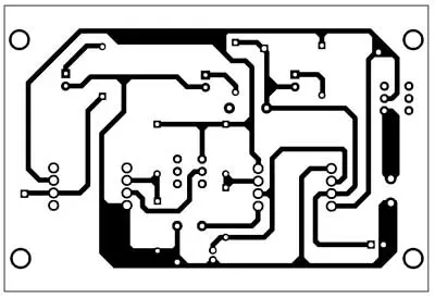
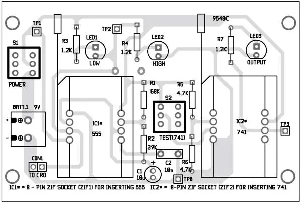
An actual-size, single-side PCB for the 555 and 741 ICs testing circuit is shown in Fig. 2 and its component layout in Fig. 3. After assembling the circuit on a PCB, enclose it in a suitable plastic box. Solder two 8-pin ZIF sockets ZIF1 and ZIF2 on the PCB for 555 timer and 741 op-amp, respectively.

Fig. 2: An actual-size PCB for the testing circuit

Fig. 3: Component layout for the PCB
During testing, both the ICs should be inserted in their respective sockets. You can check frequency output of IC1 by connecting an oscilloscope's probes to CON1 in the PCB. In case of any problem, verify that voltages at test points are as per table.
PARTS LIST | |
Semiconductors : | |
IC1 | 555 timer |
IC2 | 741 op-amp |
LED1-LED3 | 5mm LED |
Resistors (all 1/4-watt, ±5% carbon): | |
R1 | 68-kilo-ohm |
R2 | 39-kilo-ohm |
R3, R4, R7 | 1.2-kilo-ohm |
R5, R6 | 4.7-kilo-ohm |
Capacitors: | |
C1 | 10μF, 25V electrolytic |
C2 | 10nF ceramic disk |
Miscellaneous: | |
BATT.1 | 9V battery |
CON1 | 2-pin connector |
S1, S2 | On/off switch |
ZIF1, ZIF2 | 8-pin ZIF socket 2-pin terminal connector |
Test Points | |
Test point | Details |
TP0 | 0V |
Across TP0 and TP1 | 9V when switch S1 is closed |
Across TP0 and TP2 | Around 1Hz |
Across TP0 and TP3 | Around 8V when switch S2 is closed |
Author: Pankaj A. Raut

