
We are very proud of this high-resolution frequency counter, which covers a range from below 10Hz to over 2.5GHz. It has an internal timebase (naturally) but also features an external timebase input that can accept 1Hz pulses from a GPS receiver, to achieve measurement accuracy approaching that of an atomic clock! And it doesn’t cost a mint to build!
WE HAVE PUBLISHED a few digital frequency counters over the years, but they are just toys compared to this new design, which allows direct measurement of frequencies up to somewhere between 2.5GHz and 3GHz. This means it can be used to measure most of the frequencies used by Wi-Fi, mobile phones and microwave ovens.
And while high-quality commercial frequency counters often employ a temperature-compensated or oven-controlled crystal timebase, these are not in the race when compared to the very high accuracy 1Hz (lpps) signals available from many GPS receivers.
In order to make these more accurate measurements meaningful, you need a high-resolution display, which is why this new design has no less than 12 digits. Oh, by the way, because it will measure period, it can give high-resolution readout of low frequencies as well. Naturally, it uses a microcontroller and this is used in a clever way, to simplify the counting circuitry while still using high-speed logic for dealing with the UHF range up to 2.5GHz and over.
In spite of the high accuracy and resolution, this is not a difficult instrument to use. Below the 12-digit display is a row of pushbuttons, each of which has an associated LED to show when it has been pushed. The buttons are used to select one of the inputs, the mode (frequency or period), the timebase (internal or external) and the gating period (from one second to 1000 seconds).
Finally, to the right of the digital display, there are three LEDs to indicate the frequency readout in hertz or megahertz, or period in microseconds.
We will explain all these features and how to use them later on in these articles. Overall though, it’s a doddle to use.
The unit is housed in a standard plastic instrument case measuring 256 x 189 x 83mm. All components fit on two PCBs, linked by a short ribbon cable. The smaller PCB mounts behind the case front panel and supports the 12-digit display plus all of its management circuitry and components. The larger PCB sits inside the bottom of the case and supports the rest of the components and circuitry. The complete counter operates from a 9-12V DC plugpack, with a current drain of less than 650mA.
Now let’s dive into the technology used in the new design.
Block diagram
Fig.1 shows the block diagram. It’s based on a PIC16F877A microcontroller, chosen because of its reasonably large number of I/O ports - five in all, including three 8-bit ports, one 6-bit port and one 3-bit.
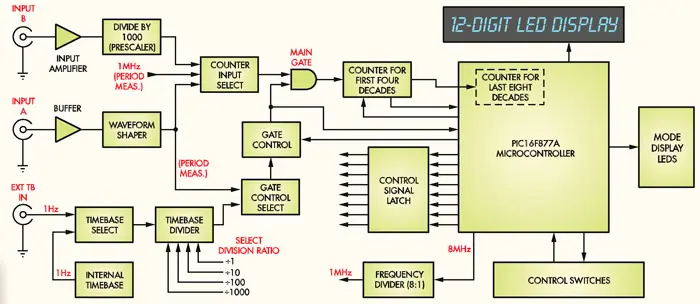
Fig.1: block diagram of the 2.5GHz 12-Digit Frequency Counter. It uses a divide by 1000 prescaler (to measure the higher frequencies) and a PIC16F877A microcontroller to process various signals and drive the display.
The PIC micro performs three important junctions. The first is to control the overall operation, in response to the settings of the pushbutton switches on the front panel. The second is to manage the counter’s 12-digit display and its associated mode and range display LEDs. Finally, it also performs some of the actual counting.
Counting of the first four ‘fast’ decades is done outside the PIC, but counting of the eight slower decades is done inside the PIC itself.
In Fig.1, the PIC is shown on the right with the 12-digit main LED display above it, the mode display LEDs to its right and the control switches below it. Although only single arrows are shown linking the PIC micro to the main LED display and the mode display LEDs, all of these are controlled via a shared multiplexing system.
To the lower left of the PIC is an 8-bit latch which is used to convey the various range and mode control signals to the counter’s input and timebase circuitry. Then at upper left of the PIC you can see the counter circuit for the first four decades, fed from the main gate and with its output passing into the PIC as input for the internal 8-decade counter.
Moving right over to the left you can see the circuit blocks for the two main counter inputs, with channel A’s input in the centre and channel B’s input above it. Note that the channel B input block includes a 1000:1 prescaler, because this is the input channel for higher frequencies (100MHz to 2.5GHz).
At lower left you’ll find the internal timebase block, the timebase selection block (internal / external timebase) and the programmable timebase divider.
Ahead of the counter’s main gate (at upper centre in Fig.1) is a block labelled Counter Input Select, which is used to select which signal is fed to the counter gate: the input signal from channel A, that from channel B, or a 1MHz signal for period measurements. The 1MHz period measurement signal is actually derived from the PIC’s 8MHz clock, via an 8:1 frequency divider (shown at lower centre, below the control signal latch).
The counter’s main gate is enabled by the PIC, but counting does not actually start until the arrival of the next rising edge of the timebase gating control signal selected by the block below it. This will either be the internal or external timebase signal, divided down by the selected ratio in the case of frequency measurements, or the signal from the channel A input in the case of period measurements.
In response to the arrival of the first leading edge of the selected gating signal, the gate control circuit will enable the main gate to begin counting, but on the arrival of the next leading edge the gate control circuit will close the gate again, to stop counting. The PIC monitors the gate control signal and when counting stops, it then proceeds to process the count (from both the four external decades and the eight internal decades) and pass it to the display.
Specifications
A digital frequency and period counter capable of making frequency measurements up to at least 2.5GHz and time period measurements to 12 digits of resolution. All circuitry is on two PCBs, linked by a short 20-way IDC ribbon cable. The counter is housed in an instrument case measuring 256 x 189 x 83mm.
Two frequency ranges: 10Hz - 100MHz (Channel A input); 100MHz - 2.5GHz or more (Channel B input; typically goes to 2.8GHz)
Period measurement range: 1 μs - 999,999 seconds (Channel A input); resolution 1μs
Input sensitivity: <20mV 0-20MHz; <75mV 20-100MHz; <250mV 100MHz+
Input channel/Mode selection: eight pushbutton switches.
Four gating periods for frequency measurement: 1s, 10s, 100s, 1000s
Corresponding resolution: 1Hz, 0.1Hz, 0.01Hz, 0.001Hz (Channel A); 1kHz, 100Hz, 10Hz, 1Hz (Channel B)
Main display: 12 x 14mm-high blue 7-segment LED displays
Mode/range indicators: 11 x 3mm LEDs
Internal timebase: Based on a 32.768kHz crystal. Accuracy approx. ±1 x 10⁻⁵
External timebase: Input for 1Hz pulses from GPS receiver, etc. Accuracy using GPS: 1Hz pulses approx. ±1 x 10-11
Input impedance: Channel A, 1MG//25pF; Channel B, 50G//3pF; External timebase, 23kG//8pF
Power source: External 9 -12V DC supply
Current drain: <650mA
Circuit details
Now let’s have a look at the full circuit. Because it is quite large, it is split into four sections: the input channels, shown in Fig.2; the timebase section (Fig.3); the main control and counting section (Fig.4) and the display multiplexing section (Fig.5).
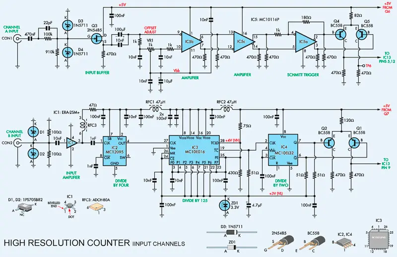
Fig.2: the input channel circuitry. Channel A handles signals up to 100MHz and is based on a 2N5485 JFET (Q3) and an MC10116P triple ECL line driver (IC5a-IC5c). IC5c’s output is then fed to Q4 and Q5, to convert it into CMOS/TTL logic. The channel B input circuitry handles signals from 100MHz to 2.5GHz. IC1 is an ERA-2SM+ broadband amplifier and this feeds IC2, an MC12095 divide-by-four ECL device. IC2 in turn feeds IC3, a programmable 8-bit ECL counter configured as a 125:1 divider. This drives IC4, an MC10EL32 ECL flipflop, which performs the final division-by-two, to bring the overall frequency division to 1000 times. The outputs from IC4 are then fed to Q1 and Q2, to again convert them to CMOS/TTL signals suitable for feeding the counter circuitry.
The upper section of Fig.2 shows the channel A input circuitry which handles signals in the range from below 10Hz to above 100MHz. This is very similar to that used in our earlier counters, with an input buffer using a 2N5485 high-frequency JFET (Q3), feeding a 3-stage waveform shaper (squarer) using an MC10116P triple ECL (emitter-coupled logic) line driver device (IC5). The square-wave output from IC5a is then passed to a logic level shifter using transistors Q4 and Q5, to convert it into CMOS/TTL logic levels to feed the counter itself.
The lower section of Fig.2 shows the channel B input circuitry, which handles signals from 100MHz to 2.5GHz.
IC1 is an ERA-2SM+ broadband amplifier device which provides a gain of around +15dB with wideband frequency choke RFC3 (an ADCH-80A) as its output load.
The amplified signals from IC1 are then fed to IC2, an MC12095 very high speed divide-by-four ECL device, which forms the first stage of the channel B prescaling divider. IC2 feeds IC3, a programmable high-speed 8-bit ECL counter configured as a 125:1 divider. It then feeds IC4, an MC10EL32 highspeed ECL flipflop which performs the final division-by-two, to bring the
overall frequency division to 1000 times. The outputs from IC4 are fed to a logic level shifter using Q1 and Q2, to convert them into a CMOS/TTL signal to feed the counter.
Timebase circuitry
Fig.3 shows the timebase circuitry. At upper left is the internal timebase generator which uses a 4060B oscillator/divider (IC6), together with a 32.768kHz crystal (X2) in the oscillator. It is followed by a 14-stage binary divider which delivers a 2Hz output signal from its O13 output (pin 3). This feeds IC7a, half of a 4518B dual 4-bit decade counter, where the 1Hz signal from the output of the first flipflop (pin 3) becomes our 1Hz internal timebase signal - fed to pin 1 of IC8a, one section of a 4093B quad Schmitt NAND gate.
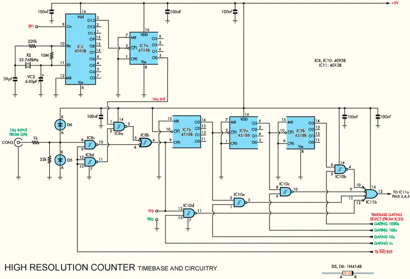
Fig.3: the timebase generator uses a 4060B (IC6) and a 32.768kHz crystal (X2) in the oscillator. IC6’s internal 14-stage binary divider delivers a 2Hz output signal from its O13 output and this feeds IC7a, half of a 4518B dual 4-bit decade counter, The resulting 1Hz signal from pin 3 is then fed to pin 1 of Schmitt NAND gate IC8a. IC7b, IC9a and IC9b operate as cascaded decade dividers, while NAND gates IC10a-IC10d are used to select either the 1Hz signal from IC8b or the output of one of the three decade dividers. The gating select signals come from the PIC via control signal latch IC23 (see Fig.4).
The external timebase signal (from a GPS receiver) arrives via CON3 and feeds IC8c, another section of the 4093B. IC8a and IC8c perform the internal/external timebase selection, under the control of a TB INT/EXT control signal from the PIC micro, which arrives at lower right in Fig.3. This signal is inverted by IC8d to enable gate IC8a when the control signal is low, but it is also applied directly to pin 9 of IC8c, to enable this gate when the control signal is high.
So a low control signal selects the internal 1Hz timebase signal, while a high level selects the external timebase signal from CON3. The outputs of IC8a and IC8c are fed to IC8b, used here as a low-input OR gate.
The remaining section of Fig.3 shows the programmable timebase divider, which uses IC7b, IC9a and IC9b as three cascaded decade dividers and the four gates in IC10 (another 4093B quad Schmitt NAND) to select either the 1Hz signal from IC8b or the output of one of the three decade dividers - all under the control of the gating select signals which come from the PIC via control signal latch IC23 (see Fig.4).
Only one of these signals is high (logic 1) at any time, so if the ‘Gating 1s’ signal is high, gate IC10d is enabled to allow the 1Hz signal from IC8b to pass through to IC11b and then to the counter’s gate control circuitry.
On the other hand, if the ‘Gating 10s’ signal is high, IC10a is enabled to allow the 0.1Hz signal from IC7b to pass through to IC11b. And the other two gating select signals work in the same way, enabling either IC10c or IC10b.
The net result is that the circuitry in Fig.3 allows the PIC to select either the internal or external timebase signals and also whether the selected signal is divided by 1, 10, 100 or 1000. The selected timebase signal emerges from pin 13 of IC11b, to feed the counter gate control circuitry.
Accuracy and resolution
Accuracy and resolution are equally important when you are making any kind of physical measurement. There’s no point in having a measuring tool that’s extremely accurate if it doesn’t provide the resolution to allow reading its measurements with the same accuracy. That’s why vernier callipers and micrometers were developed, to provide much greater length reading resolution than precision-etched steel rules.
Digital frequency counters are no exception. Since they operate by counting pulses at the input over a given period of time (the ‘gating’ period), this means that their reading resolution is inversely proportional to the gating period. With the usual gating period of one second, the resolution is clearly 1Hz.
The simplest way to achieve a higher resolution is to increase the gating period. For example a gating period of 10 seconds gives a resolution of 0.1Hz, while a gating period of 100 seconds gives a resolution of 0.01Hz and a gating period of 1000 seconds a resolution of 0.001Hz (1mHz).
So extending the gating period improves the frequency resolution. But there’s no point in doing this unless the accuracy of the counter’s timebase is high enough to make the improved resolution meaningful. That’s why a typical frequency counter using a temperature-compensated crystal oscillator as its internal timebase reference doesn’t attempt to provide a gating period of longer than 10 seconds, giving a resolution of 0.1Hz.
Nowadays, there’s a relatively easy way to provide a counter with a timebase signal that’s much more accurate than a local crystal oscillator. Many GPS receivers provide a 1pps or 1Hz signal output that is accurate to within about 1 part in 1011, because each GPS satellite contains two atomic clocks which together provide a time accuracy of better than 1 part in 1012.
If a counter uses the 1Hz pulses from a GPS receiver as its external timebase, it can therefore make meaningful frequency measurements with a gating period as long as 1000 seconds and a corresponding frequency resolution of 0.001Hz.
That’s why our new counter provides a selection of four different gating periods (1s, 10s, 100s and 1000s) and an external timebase input intended to accept the 1Hz signals from a GPS receiver. It’s also why the counter is provided with a 12-digit display, to take advantage of the higher resolution and accuracy.
Control and counting
Fig.4 covers the main control and counting sections. The PIC micro is at upper right, shown as IC22. Don’t worry too much about the righthand side of IC22 at this stage, except to note that the outputs from port B of the PIC (RB0-RB7) are brought down to connect to control switches S2-S9 and the inputs of control signal latch IC23 (a 74HC373).
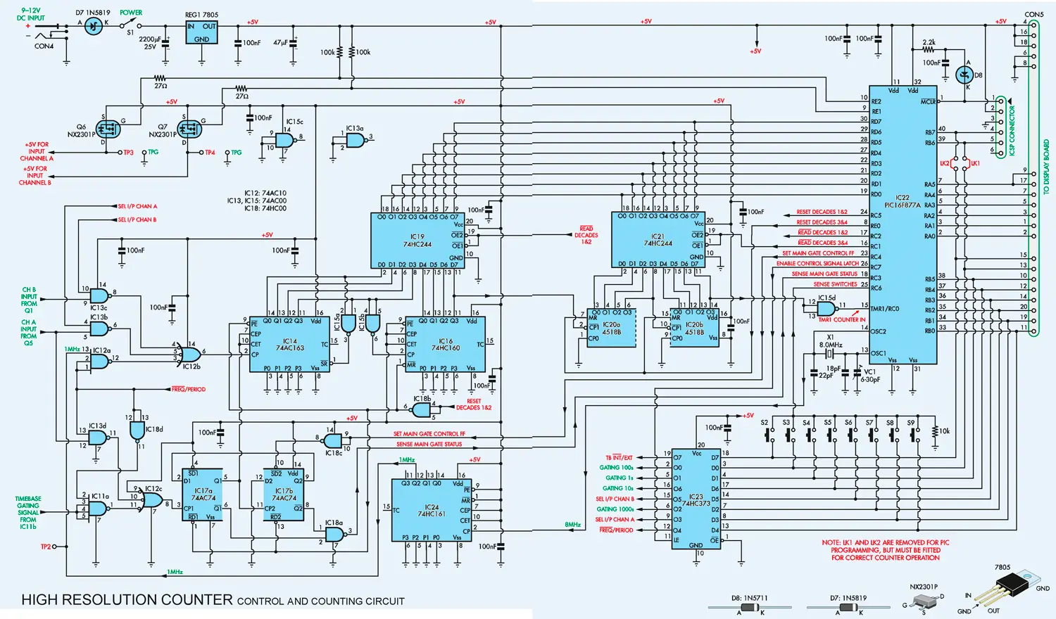
Fig.4: the PIC micro (IC22) forms the heart of the main control and counting circuit. As shown, its port B outputs (RB0-RB7) connect to control switches S2-S9 and to the inputs of control signal latch IC23 (74HC373). In operation, the PIC scans the control switches to change the input channel, timebase mode, and so on for the counter, and stores the corresponding control signals in IC23. In addition, the PIC processes the Channel A and Channel B input signals and the timebase signals (after processing via various logic gates, flipflops and counters) and drives the display board via CON5.
The PIC scans the control switches to change the input channel, time-base mode and so on for the counter and stores the corresponding control signals in IC23. As you can see, the outputs of IC23 are labelled to indicate the various control signal functions.
Just above the control switches is the PIC’s master clock circuit, based on an 8.0MHz crystal. This is entirely standard except for the addition of a 6-30pF trimcap (VC1) to allow the oscillator’s frequency to be adjusted as closely as possible to 8.00MHz. This is not for the PIC’s benefit, but because we take the 8MHz clock signal from pin 14 of the PIC and feed it down to IC24, a 74HC161 binary counter which divides it by eight to derive the 1MHz clock signal used to make the counter’s period measurements.
Note that pins 9 and 10 of IC22 (RE1 and RE2) are used to control P-channel MOSFETs Q7 and Q6 over at far left. These transistors switch the +5V power to the input circuits for channels A and B (in Fig.2), allowing the PIC to turn off the power to the channel that is not currently in use.
Below Q6 and Q7 in Fig.4 you’ll see the signals from the counter input channels (Fig.2) entering in the centre and feeding to selector gates IC13c, IC13b and IC13d. Then nearer the bottom, the timebase gating signal from IC11b (in Fig.3) enters and connects to input pins 3, 4 and 5 of IC11a.
To put things into perspective, gates IC13b, IC13c and IC12a are used to select which signal is fed to the counter’s main gate (via IC12b), while gates IC11a and IC13d below them are used to select which signal is fed to the main gate control flipflops ICl7a and IC17b (via IC12c).
In greater detail, in order to make frequency measurements, the PIC drops the FREQ/PERIOD control signal line (from pin 12 of IC23) to logic 0, which disables gate IC12a but enables gate IC11a because of the logic 1 presented to pin 2 of IC11a from IC18d (used here as an inverter). So the time-base signal selected by the circuitry in Fig.3 is able to pass through IC12c and trigger the main gate control circuit around IC17.
At the same time, the PIC raises either the SEL I/P CHAN A control signal from pin 9 of IC23 or the SEL I/P CHAN B control from pin 15 of IC23, to enable either gate IC13b or IC13c. This allows one of the two input channel signals to pass through IC12b to the counter’s main gate.
But where exactly is the counter’s main gate? It’s actually inside IC14, a very fast 74AC163 programmable synchronous 4-bit counter which we’re using here as a decade counter - the very first decade of our 12-decade counter. The counter input signal is fed into the CP input of IC14 (pin 2), while the main gate control signal from pin 5 of IC17 is fed to the CEP and CET inputs (pins 7 and 10).
So IC14 can only begin counting the input signal when IC17 ‘opens the gate’ by raising the CEP/CET inputs to a logic high.
IC14 is made to act as a decade counter by feedback applied via gate IC15a. The inputs of IC15a are connected to the ‘1’ and ‘8’ outputs of IC14, so that as soon as the count of IC14 reaches ‘9’, the output of IC15a drops and pulls the synchronous reset pin (SR, pin 1) of IC14 to logic 0. As a result, the very next pulse edge reaching the CP input of IC14 causes it to reset to ‘0’ instead of incrementing to ‘10’.
Just before we continue to follow the signal path through the counter, let’s explain how the gate control circuitry around IC17 works. Two very fast flipflops inside IC17 are interconnected in a kind of master/slave arrangement called a ‘synchroniser’. The simplest way to understand it is to follow through one operating cycle, as follows:
Before counting begins, the PIC resets both IC17a and IC17b at the same time as it resets the first two decades of the main counter (IC14 and IC16). So, to begin with, both ICl7a and ICl7b are in the reset state, with pins 6 and 8 both at logic 1 (high). As a result, pins 5 and 9 are both low, with pin 5 holding the main gate inside IC14 closed and pin 9 holding the D input of IC17a at logic 0 so that IC17a cannot switch to its set state in response to the leading edge of any timebase pulse arriving at the CP1 input (pin 3) from IC12c.
To initiate a counting sequence, the PIC provides a positive-going pulse at its RC4 output (pin 23) - which is labelled SET MAIN GATE CONTROL FF. This logic high is applied to both inputs of ICl8c, which is used as an inverter.
As a result, a negative-going pulse is applied to the SD-2 input of ICl7b (pin 10), immediately switching ICl7b into its set state with pin 9 high and pin 8 low. And since the D1 input of ICl7a (pin 2) is tied to pin 9, this effectively ‘primes’ the main gate control flipflop ICl7a.
The leading edge of the next timebase pulse to arrive at the CP1 input (pin 3) of ICl7a will immediately trigger this flipflop into its set state. This in turn drives pin 5 high and opens the main counter gate in IC14 to begin counting.
At the same time, when the Q1 output of ICl7a switches high, it also applies a clock edge to the CP2 input of ICl7b (pin 11) and since the D2 input of IC17b is tied to logic 0 (ground), this causes IC17b to switch back to its reset state with pin 9 low and pin 8 high. This causes the D1 input of IC17a (pin 2) to be pulled low as well, preparing IC17a for the final part of the cycle.
Counting then continues, but only until the next timebase pulse leading edge arrives at pin 3 of IC17a. As soon as this happens, IC17a switches back to its reset state, with Q1 (pin 5) falling back to logic 0 and closing the main gate inside IC14.
So the result of this timing control cycle is that the counter’s main gate is opened for exactly one timebase period and then closed again. And although the PIC kicks off the cycle by sending out the SET MAIN GATE CONTROL FF pulse, the actual gate timing is determined by the timebase signal applied to pin 3 of IC17a.
By the way, the PIC is able to determine when counting stops by monitoring the output of gate IC18a, which has its inputs connected to the Q outputs of IC17a and IC17b (pins 6 and 8). The output of IC18a only switches low when both Q outputs are high, which only happens at the end of a control cycle when counting stops. The output of IC18a is connected to the PIC’s RC3 input (pin 18, with the label SENSE MAIN GATE STATUS). This allows the PIC to sense when counting stops.
As already noted, IC14 contains not only the counter’s main gate, but also the first decade of the counter itself. And the next decade of counting is performed by IC16, a 74HC160 synchronous decade counter. The CP input of IC16 (pin 2) is connected to the output of IC15b (pin 6), while both inputs of IC15b (used here as a fast inverter) are connected to the ‘8’ output (pin 11) of IC14.
As a result, a positive-going clock edge is fed to the CP input of IC16 when IC14’s count falls to zero, causing IC16 to increment every time IC14 has counted 10 input pulses.
The third and fourth counting decades are based around IC20a and IC20b, two halves of another 4518B dual-decade counter. As you can see, the Q3 or ‘8’ output of IC16 (pin 11) is connected directly to the CP1 input of IC20a (pin 2), so that IC20a increments each time the count of IC16 returns to zero. Similarly, the Q3 output of IC20a is connected directly to the CP1 input of IC20b (pin 10), so IC20b increments each time the count of IC20a returns to zero.
To recap, only the first four ‘high speed’ decades of the counter are implemented in hardware external to the PIC; ie, IC14, IC16 and the two halves of IC20. The rest of the counting is done inside the PIC itself, mainly by its internal timer/counter module TMR1. This is a 16-bit timer/counter, with its input brought out to the PIC’s TMR1/RCO pin (pin 15).
Since TMR1 increments on the positive-going edge of the signal fed to pin 15, we need to invert the ‘carry over’ from pin 14 of IC20b to achieve correct counting. This is done by gate IC15d, which is connected as an inverter.
But how can we use the PIC’s TMR1 counter module to count the remaining eight decades, when as a 16-bit counter it can clearly only count to 65536 - fewer than five decades? Well, we can do so because inside the PIC we can arrange for the overflow of TMR1 (when it rolls over from 65535 to zero) to trigger an interrupt and then use a small interrupt servicing routine to increment a further 8-bit counter register every time this happens.
Doing this effectively converts the counter inside the PIC into a 24-bit counter, able to count up to 16,777,215.
Power supply and ICSP
Just before we leave Fig.4, two sections not yet mentioned are the power supply circuitry and the ICSP (in circuit serial programming) interface.
The power supply is simple, with reverse-polarity protection diode D7 in series with the front-panel power switch S1 and then a standard 7805 regulator (REG1) to provide a stabilised and filtered 5V supply for all of the counter circuitry.
The ICSP circuitry (upper right) enables the PIC to be programmed or reprogrammed with the counter firmware at any time. All the connections needed for programming are brought out to the usual 6-pin ICSP connector, while the PIC’s RB7 and RB6 pins are isolated from the rest of the counter circuit during programming by removing links LK1 and LK2.
After programming is completed, these two links are then refitted so that the counter can use RB7 and RB6 in the normal way.
Finally, note that all the connections from the PIC’s RA and RB I/O ports are brought out to 20-way DIL connector CON5, shown at far right in Fig.4. This allows the display PCB, shown in Fig.5, to be connected via a ribbon cable fitted with IDC headers.
Multiplexed display
All the displays are driven in multiplexed fashion - not just the 12 numeric digit displays, but the 11 indicator LEDs as well. The numeric displays consists of three 4-digit 7-segment blue LED displays, DISP1-DISP3, which have their common cathodes controlled by 2N7002 N-channel MOSFETs Q8-Q19. Note that only Q8-Q15 are shown, while Q16-Q19 are ‘implied’, with dotted lines. This is to save space on the diagram.
These MOSFETs are controlled by the PIC’s RA port pins via CON5 and CON6 (linked by the ribbon cable) and then through IC26 - a 4514B 4-bit-to-16-bit decoder. This circuitry thus forms the ‘digit drive’ section of the display multiplexing system.
All matching segments of the display digits are connected in parallel and driven by NX2301P P-channel MOSFETs, Q23-Q30. Again, most of these connects are shown dotted, to save space on the diagram.
These P-channel MOSFETs are controlled by the eight outputs from IC25, a 74HC240 octal buffer and line driver. This is controlled in turn by the PIC’s RB port pins, again via CON5 and CON6. So the circuitry at upper left in Fig.5 forms the ‘segment drive’ part of the display multiplexing.
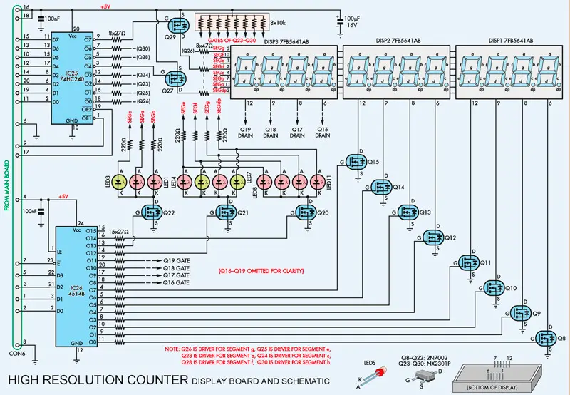
Fig.5: the displays are all driven in multiplexed fashion. As shown, the common cathodes of the three 4-digit blue LED displays, DISP1-DISP3, are switched by 2N7002 N-channel MOSFETs (Q8-Q19). These MOSFETs are controlled by the PIC’s RA port pins via CON5 and CON6 and then via IC26, a 4514B 4-bit-to-16-bit decoder. The matching display segments are connected in parallel and are controlled from the PIC’s RB port pins via IC25 (a 74HC240 octal buffer and line driver) and eight NX2301P P-channel MOSFETs (Q23-Q30). The mode and range indicator LEDs are multiplexed in similar fashion.
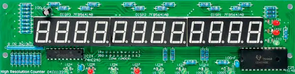
The display PCB carries the three 4-digit 7-segment LED readouts plus the various mode and indicator LEDs. The full assembly details are in Part 2, next month.
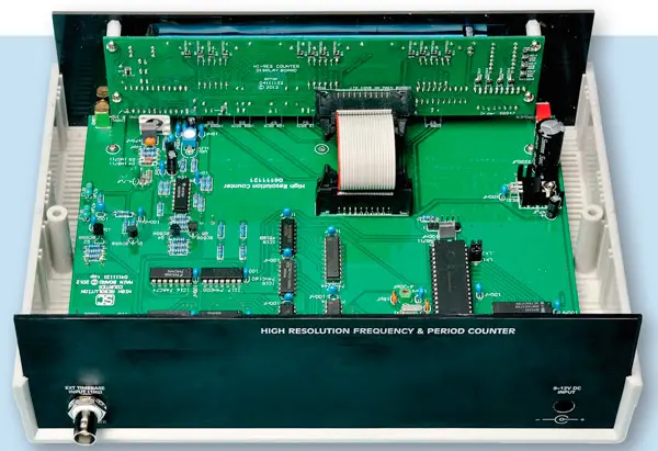
This is the view inside the completed frequency counter, from the rear. All the parts fit on two PCBs, which are linked together by a short ribbon cable. Power comes from a 9-12V DC plugpack supply.
As you can see, the 11 indicator LEDs (LED1-LED11) are part of the same multiplexing system, split into three groups forming three ‘pseudo display digits’. The three groups are controlled by MOSFETs Q20-Q22, controlled in turn by outputs O12, O13 and O14 of IC26.
The anodes of the LEDs are connected to the display segment driver lines from Q23-Q30, so they can be controlled by the PIC as part of the multiplexing. For example, LED1 is addressed as segment b of ‘digit’ 15, while LED7 and LED11 are addressed as the DP (decimal point) segments of ‘digits’ 14 and 13 respectively. As far as the PIC’s firmware is concerned, the indicator LEDs are simply specific segments of the three additional pseudo display digits.
That’s all we have space for in this first article on our new high-resolution counter. Next month, we will present the construction details for both the main PCB and the display PCB and give the set-up procedure, which is simple and straightforward.
Author: Jim Rowe