Scaling up production of 2D electronic materials
 An MIT-led group of researchers has claimed to have determined a way to make large sheets of molybdenum telluride. The team says their method is also likely to work for many similar 2D materials, and could make widespread applications in electronics feasible.
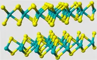
“This material has a similar bandgap to silicon and in single-layer form it has a direct bandgap,” said Lin Zhou, MIT postdoctoral researcher. “It also has strong absorption for solar radiation.” This makes Molybdenum telluride (MoTe2) key to making solar cells and transistors and it also lends itself to applications in spintronics.
MoTe2 can exist in two different forms; one is metallic, meaning it conducts electricity well, and the other is a natural semiconductor, lending itself to applications in electronics. Controlling how the material is made allows the researchers to create whichever form is needed for a particular use.
The method of creating these large sheets is based on chemical vapour deposition (CVD), and makes it possible to create sheets of any thickness, and of a size limited only by the dimensions of the CVD chamber used for deposition.
One challenge the team had to overcome was that the atoms of molybdenum telluride are weakly bound to each other, so the tendency of the two precursor materials to form molybdenum telluride is low.
The researchers were able to overcome this by using several stages of deposition, beginning with a layer of pure molybdenum. “This method makes it easy, because you only need to control one material,” Zhou explained. This step is followed by oxidation of that layer; this material is then removed and powdered tellurium is added, vaporised in a carrier gas of hydrogen and argon, at a temperature of 700°C. The use of hydrogen in the process, the team found, is crucial to producing a uniform MoTe2 film.
“Our process can grow sheets that have a very large area, are very homogeneous, and have high quality,” Zhou added.
The team now aims to explore adapting this process to create large sheets of other promising thin materials.
Author
Tom Austin-Morgan
Source: www.newelectronics.co.uk