Cool Power with D-Watt
 It has been nearly three years since we presented our last power amplifier project in Elektor - the Q-Watt Audio Power Amplifier [1]. That was a standard class AB power amplifier with high output power and low distortion. Since then a large number of audio enthusiasts have built their own copy of that amplifier. With the design presented here, we are taking the digital route for a change. In a class-D power amplifier, the output transistors operate in switching mode with a very high switching frequency. Pulse width modulation converts the amplitude of the analog input signal into a specific ratio of positive and negative pulse widths in the output signal. A filter at the output blocks the high-frequency switching signal and passes the amplified audio signal to the loudspeaker. The main advantage of this type of digital power amplifier is its high efficiency, which allows the heatsinks to be much smaller than with a comparable conventional design.
The key components in this amplifier are a driver IC in a 16-pin package and a dual power MOSFET. Together with extensive protection circuitry, they are mounted on a single PCB, so you only have to add a suitable power supply -either regulated or unregulated. There are no SMDs in the design, so building the board is very easy and you can experiment with different components or component values if you wish.
Design choices
It is possible to build a class-D amplifier entirely from discrete components, but that does not make for a simple design. Fortunately, there are several semiconductor manufacturers who make dedicated ICs for class-D amplifiers. A large variety of ICs are available for low power amplifiers, but the choice is fairly limited if you are looking for high power combined with high quality. We found an outstanding solution in the form of an IC designed by International Rectifier (now Infineon): the IRS2092. This 16-pin IC goes by the name "Protected Digital Audio Amplifier", and it integrates nearly everything you need to build a relatively simple high-performance class-D amplifier. You only have to add some power transistors.
The IC contains gate drivers that can deliver high currents for the connected power MOSFETs, a PWM modulator with built-in oscillator, bidirectional current protection and programmable dead time for driving the MOSFETs, and it can operate with switching frequencies up to 800 kHz (see the block diagram in Figure 1). Along with the datasheet [2] and a wealth of application notes, Infineon offers a lot of reference designs for the IRS2092. So why did we develop our own design when someone else has already done it for us? The answer, as you might guess, is that a practical design turns out to be good deal more elaborate than a simple copy of the reference design.

Figure 1. Block diagram of the IRS2092 digital driver IC used in this amplifier
Amplifier
With an IC designed for a specific application, it's a good idea to start with the standard application circuit from the manufacturer. That certainly holds true for the IRS2092. A detailed description of this IC can be found in application note AN-1138 [3].
Our version is shown in Figure 2, where the configuration around the driver stage IC2 and the dual MOSFET T1 is virtually "by the book". Transistor T1 is specifically designed for this sort of application, with two n-channel MOSFETs housed in a single package. The IRFI4020H-117P is a member of the Infineon family of digital audio MOSFETs and has a rated UDS max of 200 V, ID cont of 9.1 A and RDS(on) of 80 mΩ. It is a perfect choice for power amplifiers with output power of 200 to 300 W into 8 Ω. Thanks to the single package, this dual MOSFET is easy to mount on the circuit board and on a heatsink.

Figure 2. Complete schematic diagram of the D-Watt amplifier. The amplifier circuitry is shown in the top half, with the protection circuitry in the bottom half
The feedback network between the output and the input consists of R7 and R8, along with capacitor C6 to suppress RF signals (in combination with R8). The gain is determined by the ratio of R7 + R8 to R5 + R6. The input impedance of this inverting amplifier is determined by R5 and R6 and is fairly low (about 3.3 kΩ). For that reason we added a buffer stage in the form of opamp IC1A (an AD8031ANZ, which is a fast rail-to-rail opamp). You can choose which of the two inputs you want to use by fitting a jumper in the appropriate position on header JP1. The input impedance of the opamp stage is 11 kΩ. It is designed with a gain of 1, but if you wish you can increase the gain by fitting a resistor in the R3 position (A = R4/R3 + 1). The supply voltage for the opamp is provided by the ±5 V voltage regulators, which also supply the auxiliary voltages for IC2 (see below).
Virtually all of the components around IC2 have specific functions. The majority of the resistors connected to the IC determine the two current limit levels, the dead time, the bootstrap drive voltage for the high-side MOSFET, and the feedback from the output.
IC2 requires two auxiliary voltages (+5 V and -5 V). Instead of deriving them directly from the main supply voltages using Zener diodes and series resistors, we use separate voltage regulators (IC3 and IC4) to keep the auxiliary voltages stable even when the amplifier is powered from an unregulated power supply. There are Zener diodes (D4 and D5) at the inputs of the voltage regulator ICs to keep their input voltages at a safe level (the maximum allowable supply voltage is ±70 V) and reduce the dissipation of these ICs. To prevent HF switching noise from affecting the voltage regulators, additional decoupling at the auxiliary supply voltage pins of IC2 (VAA and VSS) is provided by networks in series with the supply lines (R10/C10/C11 and R11/C12/ C13). Diode D3 protects the IRS2092 if the negative supply voltage drops out. The voltage on the negative supply voltage pin VCC (which is used to drive the low-side MOSFET) is +12 V with respect to the main negative supply voltage -VP. This pin draws somewhat more current than the auxiliary supply voltage pins, so a stabilization circuit consisting of voltage regulator IC5 in series with an external Darlington power transistor (T2) is provided here. In this arrangement the transistor handles the additional power dissipation. The VCC pin of IC2 is locally decoupled by C20 and R15.
The voltage on the positive supply voltage pin of IC2 (VB), which floats relative to ground, is used to drive the high-side MOSFET. This pin is connected to a standard bootstrap circuit consisting of R16, D6 and C21, along with R21 which is necessary to charge C21 before the PWM oscillator starts running. Resistor R16 limits the peak current.
The dead time (the time interval when both MOSFETs are cut off to prevent large peak currents through both devices at the same time) can be set with voltage divider R19/R20 to one of four discrete values: 105, 65, 40 or 25 ns. Here we selected the minimum dead time setting of 25 ns by omitting R20. Note that increasing the dead time causes a significant increase in THD in the upper frequency range. You should bear in mind that MOSFETs generally need about twice as much time (or longer) to switch off than to switch on. Resistors R25 and R26 limit the charge and discharge currents to and from the gates of the power MOSFETs. The short-circuit current ratings of the driver outputs are 1 A for sourcing and 1.2 A for sinking. With a value of 18 Ω for R25 and R26, the peak charge and discharge currents are limited to about 0.5 A.
Voltage divider R17/R18 determines the low-side current limit. Here the on resistance (RDS(on)) of the MOSFETs is used for current sensing. The positive temperature coefficient of RDS(on) has the advantage that the current limit level decreases when the temperature of the MOSFETs increases. The IRS2092 has an internal 5.1 V reference voltage (VREF on pin 7) for precise setting of the current limit. Unfortunately, the drain-source resistance of MOSFETs has a fairly high tolerance. With a gate-source voltage of 10 V, the RDS(on) of the MOSFETs used here is 80 mΩ typical and 100 mΩ maximum (at 25°C). At 125°C, RDS(on) rises to more than 175 mΩ. In our design we set the current limit voltage to 1.56 V, which puts the current limit at 19.5 A (typical) at a junction temperature of 25°C. At 125°C the limit level drops to approximately 8.7 A. If the output current is too high, the IRS2092 shuts down and the LO and HO outputs are set low to protect the MOSFETs.
The high-side current limit is set using the CSH input (pin 16). This pin has a fixed threshold voltage of 1.2 V relative to VS (pin 13). For high-side current limiting, a blocking diode (D7) is necessary in addition to the voltage divider in order to protect the CSH pin against high voltage when the high side is switched off. The 0.6 V forward voltage drop over D7 increases the drain-source voltage of the high-side MOSFET by 0.6 V. Resistor R24 provides a bias voltage for D7 when the high-side MOSFET is switched on. Voltage divider R22/R23 reduces the voltage over the high-side MOSFET and D7. All this means that if you want to set the same limit level here as for the low side, you have to take D7 into account. That yields a value of 10 kΩ for R23 and 8 kΩ (adjusted to 8.2 kΩ) for R22. See the description of this amplifier on the Elek-tor Labs website [4] for the calculation. The PWM signal at the output of the MOSFETs is filtered by a second-order filter consisting of toroidal inductor LI and capacitor C29. It is followed by a Boucherot network (R28/C30), which provides an output load for the amplifier at high frequencies.
Capacitors C22-C28 decouple the supply voltages. As with all class-D amplifiers, there is a risk of power transfer from the output filter to the power supply due to the "bus pumping" effect. That mainly occurs at high signal levels and low frequencies with low load impedance. With a regulated power supply (in particular a switching power supply), this can destabilize the feedback loop. The simplest way to suppress a potential increase in the supply voltage is to connect large capacitors in parallel with the supply lines. You should start with a 10,000 μF, 100 V electrolytic capacitor on each supply line. Be careful with this, because most switching power supplies have difficulties with large capacitive loads (check the manufacturer's specifications).
The supply voltages for the amplifier are ±60 V for the 6 Ω / 8 Ω version, with 100 kΩ as the recommended value for R7. The maximum is ±70 V, but at that level the distortion increases because the PWM component of the feedback signal is stronger. If you want to use the
amplifier with a 4 Ω load, it will frequently go into current limiting with ±60 V supply voltages. In that case it is better to modify the amplifier and use different supply voltages, as described in the "4 Ω Configuration" inset.
Measured performance |
Measured with the 6/8 ft version and ±60 V supply voltages (Hypex SMPS400A400), BW = 22 kHz, R7 = 100 kft |
• Input sensitivity: | 1.3 V (189 W / 8 Ω, THD+N = 1%) 1.25 V (174 W / 8 Ω, THD+N = 0.1%) |
• Input impedance: | 3.33 kΩ / 11 kΩ |
• Continuous output power: | 174 W into 8 Ω (THD+N = 0.1%, 1 kHz) 189 W into 8 Ω (THD+N = 1%, 1 kHz) 224 W into 6 Ω (THD+N = 0.1%, 1 kHz) 246 W into 6 Ω (THD+N = 1%, 1 kHz) |
• Power bandwidth: | 5 Hz (-3 dB) to 20 kHz (-1 dB) |
• Slew rate: | 15 V/μs (8 Ω) |
• Rise time: | 4.4 μs (8 Ω) |
• Signal to noise ratio: (reference 1 W / 8 ft) | >77 dB (linear, BW = 22 Hz to 22 kHz) >80 dBA |
• Total harmonic distortion plus noise: (BW = 22 kHz) | 0.014% (1 kHz, 1 W / 8 Ω) 0.004% (1 kHz, 50 W / 8 Ω) 0.024% (1 kHz, 1 W / 6 Ω) 0.0046% (1 kHz, 50 W / 6 Ω) |
• Intermodulation distortion: (50 Hz / 7 kHz, 4:1) | 0.013% (1 W / 8 Ω) 0.023% (50 W / 8 Ω) 0.013% (1 W / 6 Ω) 0.017% (50 W / 6 Ω) |
• Dynamic IM distortion: (3.15 kHz square wave / 15 kHz sine wave) | 0.037% (1 W / 8 Ω) 0.009% (50 W / 8 Ω) 0.043% (1 W / 6 Ω) 0.008% (50 W / 6 Ω) |
• Damping factor: | 174 (1 kHz, 8 Ω) |
• Efficiency at full power: (THD+N = 0.1%) | 93% with 8 Ω load 94% with 6 Ω load |
• DC protection: | +3 V / -4 V |
• DC output offset: | <0.3 mV |
• Switch-on delay: | 6 s |
Protection
To supplement the built-in protection of the IRS2092, we added a number of external protection circuits: overvoltage protection for both supply voltages, undervoltage protection (also for both supply voltages), and DC protection with switch-on delay. Each of these protection circuits can deenergize the output relay and shut down the IRS2092. The DC protection circuit ensures that the output is switched off if the DC voltage at the output is too high, in order to protect the connected loudspeaker. The DC protection circuit reacts at a DC level of a few volts. A relatively high value was chosen for this because there is always some DC voltage present at the output when no load is connected and the IRS2092 is shut down. Apparently there is a leakage current from the VS pin when the IRS2092 is in shutdown mode.
The DC protection circuit consists of R38, R39, R40, C34, T6 and T7. Voltage divider R39/R40 determines the trip levels. With the indicated resistor values, they are + 3 V and -4 V. Although the selected levels are somewhat higher than usual, they should not be harmful to the loudspeaker system. When T6 or T7 starts conducting due to excessive DC voltage, it drives T5 into conduction, which in turn switches on T4. That transistor discharges capacitor C35, cutting off MOSFET T8 and causing the relay to drop out. At the same time, the IRS2092 is shut down by discharging C14 on the CSD pin through T3, which acts as a level adapter. Diode D11 near T5 is included to prevent T3 from being constantly driven in to conduction through R35.
The relay is driven by a small MOSFET so that the value of capacitor C35 (which together with R41 provides the switch-on delay) can be kept small. That also allows C35 to discharge faster through T4. Header JP2 is provided for testing the DC protection circuit. For normal operation the jumper is placed in the "Amp." position here. If you want to try a different value for R40 in order to change the DC trip level, put the jumper in the "Ext. DC Test" position so you can use an external adjustable DC voltage source.
The maximum continuous drain current of the IRFI4020H-117P dual MOSFET used here is 9.1 A with a case temperature of 25°C. At a temperature of 100°C it is only 5.7 A. For this reason, we added supplementary overvoltage protection to limit the power dissipation at relatively high supply voltages. This amplifier is designed for maximum supply voltages of ±70 V. The overvoltage protection is dimensioned to react at about ±75 V. The main components here are the two Zener diodes D15 and D16. Depending on the values of series resistors R52 and R53, transistor T12 starts to conduct when the positive or negative voltage is too high. It drives transistor T5 into conduction (the same as for DC protection), which causes the relay to be de-energized through T4 and T8. Diode D17 is necessary for detection of positive overvoltage. Without D17 the voltage on the emitter of T12 would rise in an overvoltage situation, but that would not cause the transistor to start conducting.
Undervoltage detection is a bit more complicated, and it additionally ensures that the relay is de-energized immediately when the amplifier is switched off in order to prevent popping sounds from the loudspeaker. Here two transistors are used for voltage detection, instead of two Zener diodes. Transistors T10 and T11 both conduct when the two supply voltages are high enough, causing T9 to be cut off. Otherwise T9 is driven into conduction and the relay is de-energized through T5, T4 and T8 as previously described. Diode D14 prevents T11 from conducting when T10 is fully conducting. In that situation the voltage on the collector of T10 is about -0.6 V, and without D14 the emitter of T11 would also be at that level, so it would also start conducting at a very low supply voltage level. That would impair the operation of the undervoltage protection circuit. The detection levels are determined by voltage divider R49/R50 for the positive supply voltage and voltage divider R47/R46 for the negative supply voltage. The values of R49 and R47 also depend on the base current of T11 and the emitter current of T10. With the values shown on the schematic diagram, the undervoltage protection will react when the supply voltages drop below about ±40 V.
Component List |
Resistors Default: 5%, 0.25W
R1,R8 = 1kΩ
R2,R23,R24,R30,R34,R36,R37,R46,R50,R54 = 10kΩ
R3,R20 = not mounted
R4 = 2kΩ 1%
R5 = 330Ω
R6,R18 = 3kΩ 1%
R7,R52 = 120kΩ
R9 = 470Ω
R10,R11,R15,R31 = 10Ω
R12,R13 = 1.8kΩ, 2W
R14 = 2.2kΩ
R16 = 4.7Ω
R17,R35 = 6.8kΩ
R19 = 5.6kΩ
R21 = 33kΩ
R22 = 8.2kΩ
R25,R26 = 18Ω
R27 = 1Ω, 1 W
R28 = 10Ω 1W
R29 = 2.2kΩ, 2W
R32,R40 = 4.7kΩ
R33,R43 = 15kΩ
R38,R39,R45,R48,R51 = 22kΩ
R41 = 1MΩ
R42 = 10MΩ
R44 = 2.7kΩ
R47 = 150kΩ
R49 = 820kΩ
R53 = 47kΩ
P1 = 1kΩ trimpot, top screw adjustment Inductor L1 = 22μH, Micrometals type T130-2 ring
core, max. 20x40mm. Wire: 200cm of
1.5mm/AWG15 enameled copper Capacitors C1,C5,C7,C8,C9 = 1nF 1%, 63V, polystyrene, 7.18mm pitch (LCR Components type EXFS/HR 1000pF ±1%)
C2,C3,C11,C13,C16,C18,C31 = 100nF 10%, 50V, X7R, 0.2’’ pitch
C4 = 10μF 10%, 63V, MKT, 15mm pitch
C6 = 150pF 5%, 500V, silver mica, 5.9mm pitch (Cornell Dubilier type CD15FD151JO3F)
C10,C12,C14,C20,C32 = 10μF 20%, 50V, 5x11 mm, 2mm pitch
C15 = 10nF 10% 100V, X7R, 0.2’’ pitch
C17,C19,C33 = 1μF 20%, 50V, 5x11 mm,2mm pitch
C21 = 22μF 20%, 50V, 5x11 mm, 2mm pitch
C22,C24 = 100nF 10%, 250V, MKT, 4x10 mm, 7.5mm pitch (TDK type B32520C3104K000)
C23,C25 = 680μF 20%, 100V, 28mΩ @ 2.57A, 18x40 mm, 7.5mm pitch (Rubycon type 100ZL680MEFC18X40)
C26 = 100nF 10%, 200V, X7R, 0.2’’ pitch (Kemet type C330C104K2R5TA)
C27,C28,C30 = 100nF 5%, 400V, polypropylene, 15mm pitch (TDK type
B32652A4104J000)
C29 = 470nF 5%, 400V, polypropylene, 15mm
pitch (TDK type B32652A4474J000)
C34 = 100μF 20%, 10V, bipolar, 2.5mm or 3.5mm pitch, diam. 8mm max.
C35 = 2.2μF, 50V, 5x11 mm, 2mm pitch | Semiconductors D1,D2,D11,D13,D14,D17 = 1N4148
D3,D8,D9 = 1N4007
D4,D5,D10 = BZX85C18 SB00018/E1,18V/1.3W zener diode
D15,D16 = BZX55C68-TR, 68V/0.5W zener diode (alternatively, NXP type BZX79-C68)
D6 = MUR120G (200V, 1A)
D7 = BAV21 (250V, 250mA)
D12 = LED, green, 3mm
T1 = IRFI4020H-117P
T2 = TIP122G
T3,T4,T6,T7,T9,T10,T11,T12 = BC547C
T5 = BC557C
T8 = IRFD210PBF
IC1 = AD8031ANZ
IC2 = IRS2092PBF
IC3 = MC7805CTG IC4 = MC7905ACTG
IC5 = MC7812CTG Miscellaneous K1,K2,K3,K4,K5 = Faston spade connector,
PCB mount, dim. 6.35x0.81 mm, 0.2’’ pitch
JP1,JP2 = 3-pin pinheader, 0.1’’ pitch, with jumpers
RE1 = relay, PCB mount, SPCO, 16A,
48V/5.52kΩ (TE Connectivity/Schrack type
RT314048)
HS1 = heatsink, PCB mount, 2.6K/W, mounting
pins spaced 1 inch (Aavid Thermalloy
type 530002B02500G)
Heatsink for IC4/IC5/T2: 27x90 mm aluminum
sheet, 2mm thick
Heatsink for IC3: 30 x 30 mm aluminum
sheet, 1mm or 2mm thick
Isolation materials for T2,IC3,IC4,IC5 (TO-220
thermal pad + TO-220 bush)
6 pcs solder pin, 1.3mm diam.
1 pc DIP-16 IC socket
1 pc DIP-8 IC socket
Kit of parts incl. PCB 150115-1 (mono), excl.
supply: Elektor Store # 150115-71
PCB # 150115-1, available separately and
optionally Ancillaries for Hypex SMPS400A400 PSU connection 1 pc JST VHR series 5-way straight case for PCB connector, 3.96mm pitch (RS Components
# 820-1188, set of 5 pcs)
1 x JST VHR series 3-way straight case for PCB connector, 3.96mm pitch (RS Components # 820-1175, set of 5 pcs)
5 x JST cable set with crimp connectors at both sides (RS Components # 820-1135, set
of 5 pcs)
3 pcs isolated Faston connector, female, 0.25’’ pitch |
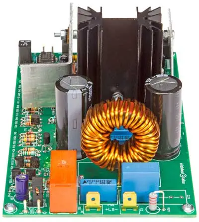
Construction: three heatsinks and a coil
Figure 3 shows the printed circuit board for the D-Watt amplifier. Although it may seem fairly large, all necessary heatsinks are also located on the board, so there is no need to add a bulky external heatsink. Furthermore, all the components are leaded types, so building the board is straightforward and you can easily experiment with various modifications if you wish.

Figure 3. The printed circuit board for the D-Watt amplifier
The bare PCB is available in the Elektor Store, but you can also buy a semi kit (order number 150115-71) containing the PCB and all necessary components, including the heatsinks (note that you will have to drill the holes in the heatsinks yourself).
Not much needs to be said about mounting most of the components; they should not present any difficulties if you have a reasonable level of soldering experience. Do not mount T1 right away.
Use good-quality sockets for IC1 and IC2, preferably with turned pins. It is important to use capacitors of the best possible quality for the PWM modulator circuitry and HF decoupling of the audio input signal (C1, C5, C7, C8 and C9). For that reason we provided lots of room for these components on the PCB, so you can decide for yourself whether you want to mount polystyrene, polypropylene or ordinary polyester types. For HF decoupling of the feedback network (C6), we specifically recommend using a high-quality silver mica capacitor (150 μF / 500 V). Using a different type here is not advisable. For coupling capacitor C4 at the input we used a standard MKT type. Polypropylene is not desirable here due to the large component size, which would cause the capacitor to pick up too much noise (including switching noise).
Voltage regulator IC3 only needs a small heatsink, which you can make yourself from a piece of aluminum sheet with a thickness of 1 mm. An area of 30 x 30 mm is sufficient. The metal mounting tab of the IC is connected to ground, so the IC does not need to be insulated from the heatsink. Mount the heatsink plate on the voltage regulator so it is a few millimeters above the surface of the board. Also make sure that the mounting hole in the corner of the board remains accessible (see Figure 4). IC4, IC5 and T2 are all mounted on an aluminum plate 2 mm thick with dimensions of 27 x 90 mm, with one end bent at a right angle 65 mm from the end (see Figure 4 again). To avoid contact with other components, mount the heatsink on these three components so it is at least 5 mm above the surface of the board. All three components must be insulated, and two of them (IC5 and T2) are mounted opposite each other and secured by the same screw. The two holes in the plate are spaced exactly 40 mm apart, and IC4 is located 14 mm from the edge of the board. You will have to determine the height of these two holes by empirical measurement.

Figure 4. Two of the heatsinks are home-made from aluminum sheet metal with a thickness of 1 mm or 2 mm, respectively. The small one is for IC3, and the large on is for IC4, IC5 and T2
Next we have the heatsink for T1. The package of this dual MOSFET is completely composed of plastic, so it does not need to be insulated. First mount the heatsink on the PCB, then apply a thin coat of thermal grease to the rear of T1 and insert its leads into the corresponding holes in the board. Secure T1 to the heatsink with a screw, plain washer, split washer and nut (screw length 12 mm). First check that the leads are properly positioned in the holes without twisting, and then tighten the screw firmly. After this, solder the MOSFET leads to the PCB.
Output inductor
The most difficult component in this project (in terms of construction) is the inductor of the output filter. You have to wind it by hand on a toroidal core with a diameter of 33 mm (1.3 inch) using 1.5 mm enameled copper wire (15 AWG). The core is an iron powder type from Micrometals. We chose this core for its linear characteristics, so that the filter does not cause much distortion. The downside of this core material is its low permeability, which means a lot of turns have to be wrapped on the core to obtain the necessary inductance.
You need 2 meters (approx. 7 feet) of 1.5 mm enameled copper wire (15 AWG) for the winding, and you have to wind 45 turns on the core. They will not fit in a single layer on the inner circumference of the core, so the coil must be wound in a special way to keep the parasitic capacitance low. The turns of the second layer of the winding are placed on top of the turns of the first layer on the inner circumference of the core. On the outer circumference, the turns of the second layer are placed next to the turns of the first layer. The turns of the third layer are placed next to the turns of the first layer on the inner circumference, and next to the turns of the second layer on the outer circumference. Repeat this procedure for the fourth layer. After you have wound 45 turns on the core this way, the ends of the copper wire will be located opposite each other on either side of the core. You may have to improvise or make a few adjustments to get all 45 turns on the core this way, but hopefully you understand what we mean. Have a look at the picture of the finished coil in Figure 5. We should warn you that 1.5 mm copper wire (15 AWG) is fairly stiff and not easy to bend. Work carefully and wind the wire as tightly as possible against the core, but do not use any metallic tools due to the risk of damaging the insulation of the wire.

Figure 5. To keep the parasitic capacitance as low as possible, 45 turns of copper wire have to be wound on the core in a specific manner
When you are done, you will have a coil with an inductance of 22 μH and a resistance of about 20 mΩ. Now you can mount it vertically on the PCB and solder it in place.
That completes the assembly of the circuit board.
Some measured characteristic curves Test equipment: Audio Precision System Two Cascade Plus 2722 Dual Domain (Elektor Audio Lab) |
Plot A This shows the measured amplitude versus frequency with load impedances of 4, 6 and 8 Ω. In the 20 kHz region the curves show that the dimensioning of the output filter is a good compromise for the different impedances. The deviation from 10 to 20 kHz is approximately ±1 dB. With 8 Ω (cyan) the resonant frequency of the output filter is clearly visible. With 6 Ω (green) the curve is nearly flat, and with 4 Ω (blue) the corner frequency is somewhat lower. | 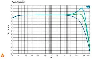 |
Plot B THD+N at 1 W and 50 W with an 8 Ω load and measurement bandwidths of 22 kHz and 80 kHz, respectively. Measurements with large bandwidth are usually not shown in data sheets for class-D power amplifiers because the effect of the switching frequency increases with greater bandwidth. However, the amplifier does produce output signals above 22 kHz, so showing what happens above that frequency is only fair, even if you cannot hear it. The red curve shows the THD plus noise at 50 W, measured with a bandwidth of 22 kHz. The blue curve was measured at the same power level but with a measurement bandwidth of 80 kHz. The cyan curve shows the THD plus noise at 1 W with a bandwidth of 22 kHz, and the yellow curve show the THD plus noise at 1 W with a bandwidth of 80 kHz. All measurements were made using a ninth-order elliptical low-pass filter with a corner frequency of 200 kHz ahead of the analyzer input to block residual PWM noise from the amplifier. | 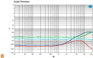 |
Plot C FFT of a 1 kHz signal at 1 W into 8 Ω. Hardly any harmonics are visible, although the second harmonic can be seen in the noise of you look closely. The TDH+N is 0.014% and consists almost entirely of noise. In this FFT plot and the next one, the switching frequency of the Hypex power supply is clearly visible at 90 kHz (according to the manufacturer’s datasheet, it ranges from 80 to 120 kHz), but the level is so low (–82 dB) that it is not a cause for concern. | 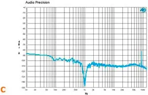 |
Plot D The same FFT measurement as plot C, but with a power level of 50 W into 8 Ω. Here some harmonics are visible. The THD+N is 0.004%, and the switching noise from the power supply has dropped to an insignificant level of –96 dB. | 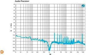 |
Plot E THD+N versus output power (1 kHz / 8 Ω, BW = 22 kHz). The measurement bandwidth was reduced here to improve the visibility of the distortion curve. The distortion gradually increases above approximately 50 W. The amplifier can comfortably deliver 200 W with the nominal supply voltages. | 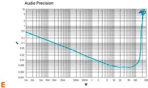 |
4 Ω Configuration If you want to use the amplifier with a 4 Ω load, we recommend using a different
MOSFET type for T1: the IRFI4212-117P. In addition, the maximum supply voltages in that case are ±46 V. Several other small modifications are also necessary. To start with, the current limit value must be raised by setting R17 to 6.2 kΩ, R18 to 3.9 kΩ and R22 to 12 kΩ. That makes the current limit level 15.33 A with a 3-Ω load. Now the 48 V relay can be connected directly to the power source, with R44 replaced by a wire link. The feedback network must also be modified by reducing
the value of R7 to 75 kΩ. At continuous full output power with a 3-Ω load, current limit protection will trip after a few seconds because the temperature of the main heatsink will rise too much, despite the high efficiency. With this configuration it can therefore be a good
idea to make a larger heatsink yourself (no higher version is available for the type
specified in the components list). Extensive measurement data for the 4-Ω configuration is available on the Elektor
Labs website [4]. Among other things, it shows that the amplifier can deliver 243 W into 4 Ω with 1% distortion (and even 297 W into 3 Ω). |
Power supply and enclosure
Next you have to fit the board and its power supply into a suitable enclosure. Although it is possible to use a conventional power supply with a hefty power transformer, bridge rectifier and filter capacitors, that doesn't really fit with a modern class-D amplifier. Furthermore, the measured performance of the D-Watt Amp is significantly better with a regulated power supply. For that reason, we used switching power supplies from the Dutch company Hypex in our prototype. They are specifically designed for use with class-D power amplifiers. We chose the SMPS400A400, which can supply 400 W at 20 Hz with nominal output voltages of ±64 V (the mains voltage in our lab is a bit lower than usual, so we measured output voltages of ±60 V). With this power supply the amplifier is suitable for loads from 6 to 8 fi. For lower load impedances it advisable to modify the amplifier (see the inset), as otherwise the protection circuit will trip occasionally during high-power passages.
In Figure 6 you can see how we fitted two amplifier boards and two Hypex power supplies into a standard enclosure. There is not much wiring in the enclosure because everything is located on a single PCB.

Figure 6. Two amplifier boards and two switching power supplies fitted in an enclosure
We hope you enjoy building and using this cool high-power amplifier. More detailed information about the amplifier, along with even more measurement data, is available on the Elektor Labs website [4].
Web Links
[1] www.elektormagazine.com/magazine/elektor-201309/23330
[2] www.infineon.com/dgdl/irs2092.pdf?fileld=5546d462533600a401535675flbe2790
[3] www.infineon.com/dgdl/an-l 138.pdf?fileld = 5546d462533600a40153559a077610dl
[4] www.elektormagazine.com/labs/200w-class-d-audio-power-amplifier-150511
Author: Ton Giesberts (Elektor Labs)