
MIT’s twin PUF: two chips sharing a unique physical fingerprint for direct authentication
Researchers at MIT have developed a groundbreaking CMOS fabrication technique that enables two chips to share a unique physical “fingerprint”, allowing them to authenticate each other directly without storing secret keys on third-party servers. The new “twin PUF” method significantly improves hardware security, privacy, and energy efficiency for edge devices and IoT systems.
MIT’s twin PUF: two chips sharing a unique physical fingerprint for direct authentication
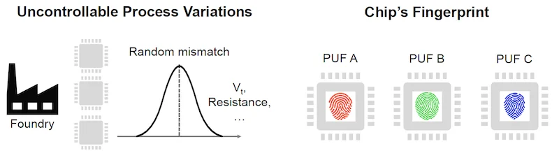
During wafer processing (before dicing), specially designed transistor structures are placed along the edges of two adjacent dies and connected via metal layers. On-chip photodiodes harvest energy from LED illumination to power the circuit. This energy induces controlled gate-oxide breakdown in selected transistors. Because of natural manufacturing variations, the breakdown times differ randomly, creating unique electrical states - the PUF fingerprint.
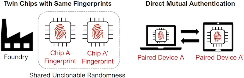
In the twin configuration, four transistors (two on each chip) share the same breakdown event, resulting in complementary but perfectly matched responses. After dicing, the two chips form a matched pair with correlated randomness, similar to tearing a piece of paper in half where the edges match uniquely.
Fabrication process: shared gate-oxide breakdown powered by photovoltaic energy from LED
Traditional PUF vs MIT Twin PUF: removing server dependency
The technology is especially promising for:
This approach brings hardware security closer to the physical layer, making cryptographic schemes more robust and suitable for resource-constrained environments.
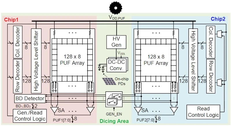
Prototype: 128 × 8 PUF cell arrays fabricated in 65-nm CMOS