Near-field probes are essential tools for engineers working with electromagnetic compatibility (EMC). They allow precise detection of unwanted electromagnetic emissions directly on printed circuit boards (PCBs).
What Are Near-Field Probes?
Near-field probes are small antennas designed to measure electromagnetic fields very close to a signal source. Unlike far-field antennas, they capture localized electric or magnetic fields without being affected by distant radiation.
These probes are typically connected to a spectrum analyzer or oscilloscope to visualize frequency and amplitude behavior.
Types of Near-Field Probes
There are two main categories of near-field probes:
- Magnetic field probes - sensitive to current flow and loop radiation
- Electric field probes - detect voltage-related emissions
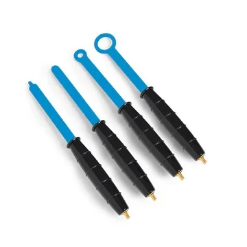
Figure 1. A near-field probes kit.
Magnetic probes are commonly used for tracking high-frequency noise paths, while electric probes help identify voltage coupling issues.
How Near-Field Probes Are Used
Engineers use near-field probes to scan PCBs, cables, and connectors to locate emission hotspots. By moving the probe across the surface, it is possible to identify problematic components or traces.
This approach is especially valuable during early development stages, when design changes are still easy and inexpensive.

Figure 2. EMC tape used to shield electronic devices
Benefits in EMC Troubleshooting
Near-field probing provides immediate feedback and helps reduce guesswork in EMC debugging. It allows engineers to:
- Locate sources of electromagnetic interference
- Compare emissions before and after design changes
- Reduce time spent on compliance testing
Although near-field measurements are not standardized compliance tests, they are extremely effective for relative comparison and diagnostics.
Conclusion
Near-field probes are powerful diagnostic instruments for identifying and resolving EMC issues. When used correctly, they significantly improve design quality and reduce costly redesign cycles.