The 40-EL4216-PWE1XG power supply unit (PSU) made by TCL (factory designation EL42E1C6/EL42E1C7) is used in 32-, 37-, 40- and 42-inch TCL LCD TVs with LED backlight, as well as in TVs sold under the ERISSON, MYSTERY, THOMSON and other brands. It generates regulated 115 V, 12 V and 3.3 V outputs, and the integrated LED driver produces the VLED voltage for the LCD panel backlight. This article covers the TEA1755 PFC/flyback controller pinout, the operation of the OZ9902C LED driver and step-by-step troubleshooting of typical PSU faults.
The full schematic diagram of the 40-EL4216-PWE1XG power supply (Fig. 2 and Fig. 5) is available in high resolution in the service manuals archive: download the TCL 40-EL4216-PWE1XG power supply schematic.
TEA1755 PFC and flyback controller
The TEA1755 pinout (SO16 package) is given in Table 1.
The PFC controller operates in QR or DCM mode; the maximum PFC switching frequency is limited to 139 kHz to reduce switching losses. If necessary, one or more switching cycles are skipped to keep the frequency below 139 kHz.
The PFC uses a dual boost architecture with two output voltage levels depending on the mains input voltage range.
The dual boost output is controlled by an internal 8.1 µA current source together with the VOSENSE input, which senses the PFC output voltage. The mains input voltage is sensed at pin 7 (VINSENSE) through the RD1-RD8, R301, R339 divider to control the internal current source. At low mains voltage the current source is on and the PFC output is low, 250 V (typical); at high mains voltage the current source is off and the PFC output is high, 385 V DC.
The PFC output voltage is regulated by an error amplifier (VOSENSE input). The voltage is compared with a 2.5 V reference, the error is converted into a current at the PFCCOMP output, and the voltage at this pin together with the VINSENSE voltage determines the PFC on-time.
At initial start-up the flyback converter starts at maximum output power in quasi-resonant (QR) mode. As the output power decreases from maximum to minimum, the controller passes through four operating modes: QR, DCM, frequency reduction (FR) and burst mode (BM) (see Fig. 4).
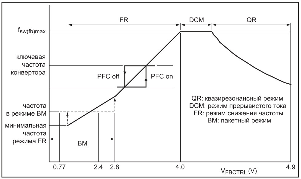
Fig. 4. Converter operating modes
The internal demagnetization detection and MOSFET valley switching circuit is active in all four modes. In QR mode the circuit operates at high and maximum power, which is regulated by limiting the peak current of the power MOSFET. As the power decreases, the switching frequency rises until it reaches the maximum (139 kHz); a further power decrease causes a transition to discontinuous conduction mode (DCM). In these modes the voltage at the VFBCTRL feedback input (derived from the 12 V and 115 V secondary outputs by the U401 (TL431) shunt regulator and fed to U301 via optocoupler PC1) is in the 4…4.9 V range. Below 4 V the circuit enters frequency reduction (FR) mode, in which the power is reduced by lowering the converter switching frequency while the peak current stays constant. When the PFC output current drops to 25 % of nominal, the PFC is switched off, which improves overall efficiency at low output power. Increasing the output power from minimum to maximum restarts the PFC. More details on the operation of this IC in all modes can be found in [1, 2].
Table 1. TEA1755 pinout (SO16 package)
| Pin | Name | Function |
|---|---|---|
| 1 | VCC | IC supply voltage: Vstartup=22.3 V; Vth(UVLO)=13.4 V. At power-up the capacitor connected to this pin is charged to Vstartup by the internal high-voltage current source. When VCC <0.6 V, the charging current is limited to 1.1 mA; this prevents IC overheating if the VCC pin is shorted. Between 0.6 V and Vth(UVLO) the charging current is 5 mA for fast start-up. When Vstartup is reached, the high-voltage current source is switched off and VCC is regulated at Vstartup until the converter starts |
| 2 | GND | Ground |
| 3 | FBCTRL | Feedback input for direct connection of the feedback optocoupler. 4.9 V at the input gives maximum output power. At 4 V the flyback converter switches to frequency reduction (FR) mode; burst mode is entered at 1.2 V and exited at 2.8 V. The converter driver is switched off below 0.77 V. The built-in logic controls an internal 29 µA current source connected to this pin, which can be used to implement a time-out function for detecting an open control loop or a shorted output. The time-out function is disabled by connecting a 180 kΩ resistor between this pin and ground |
| 4 | FBAUX | Input from the transformer auxiliary winding for demagnetization detection, overpower protection (OPP) and overvoltage protection (OVP) of the flyback converter. The combination of demagnetization detection and valley detection at the HV pin determines the flyback turn-on moment. Converter OVP is detected at a current above 300 µA into FBAUX; OPP is detected at a current below 100 µA at this pin |
| 5 | LATCH | General-purpose latched protection input. When Vstartup is reached (at VCC), the LATCH voltage rises to 582 mV before the PFC and flyback controllers are enabled. Latched protection is triggered when the voltage drops below 494 mV, and the PFC and converter are switched off. The logic controls an internal 30.5 µA current source connected to this pin, so an NTC thermistor can be connected directly for overtemperature protection |
| 6 | PFCCOMP | Frequency compensation network for the PFC control loop |
| 7 | VINSENSE | Mains voltage sense input with six functions: – mains start level (brown-in): Vstart=1.16 V; – mains stop level (brown-out): Vstop=0.89 V; – mains voltage compensation of the PFC control loop gain bandwidth; – fast latch reset level: Vflr=0.75 V; – dual boost switching point: Vbst(dual)high=2.28 V or Vbst(dual)low=2.08 V; – standby: Vth(pd)=385 mV; – exit from standby: Vth(pd)=460 mV |
| 8 | PFCAUX | Input from the PFC inductor auxiliary winding for demagnetization timing and valley detection to control PFC switching. For EMI protection the winding is connected through a 5 kΩ resistor |
| 9 | VOSENSE | PFC output voltage sense input with several functions: – open-loop and short-circuit detection: Vth(stop)=1 V; – initial start level: Vth(start)=1.1 V; – output voltage regulation: Vreg=2.5 V; – soft PFC OVP (cycle-by-cycle regulation): Vovp=2.62 V; – PFC output voltage control output; dual boost current: Ibst(dual)=–8.1 µA |
| 10 | FBSENSE | Flyback converter current sense input. This pin senses the sum of the voltages across three resistors; choosing them correctly allows to: – minimize the risk of converter transformer saturation; – correctly set PFC turn-on and turn-off; – make the system work independently of the mains voltage. Voltage levels Vsense(fb)max=545 mV and Vsense(fb)min=232 mV; the second level is the regulated peak transformer current used in burst mode or frequency reduction mode. Two internal current sources are connected to this pin: – Istart(soft)fb=60 µA for converter soft start; – Iadj(FBSENSE)=2.1 µA to support PFC on/off adjustment |
| 11 | PFCSENSE | PFC overcurrent protection input (cycle-by-cycle). The PFC power MOSFET is switched off when VPFCSENSE reaches 495 mV. For soft start and soft stop an internal 60 µA current source is connected to this pin to prevent audible noise. A soft-start resistor of at least 15 kΩ is required |
| 12 | PFCDRIVER | Gate driver output for the PFC MOSFET |
| 13 | FBDRIVER | Gate driver output for the flyback MOSFET |
| 14 | PFCTIMER | Timer pin with two options: 1. The timer delays PFC switch-off when the converter is switched off or its load decreases. The PFC is switched off when two conditions are met: – the feedback switching frequency is below 53 kHz (only in FR mode); – high voltage at PFCTIMER (≥ 3 V). 2. When an external supply is connected to this pin, the PFC is forced on at ≤ 1.03 V and switched off at ≥ 4.4 V |
| 15 | HVS | High-voltage safety spacer, not connected |
| 16 | HV | High-voltage input for the internal start-up current source (output to VCC) and valley detection; demagnetization detection at FBAUX combined with valley detection at HV determines the turn-on moment of the flyback MOSFET |
The PFC (QW1) and converter (QW2) power switches are MDF12N50 (N-MOSFET, VD=500 V, ID=11.5 A, RDS(ON)=0.65 Ω) and AP09N70I (N-MOSFET, VD=650 V, ID=9 A, RDS(ON)=0.75 Ω) respectively.
The 115 V and 12 V secondary outputs use ultrafast rectifier diodes U808F (VR=800 V, IF=8 A) and R20150 (VR=150 V, IF=20 A) respectively.
The standby power module derives 3.3 V from the 12 V rail to supply the standby microcontroller on the TV main board.
The 12 V rail is fed to the main board through the U405 MOSFET switch (AOZ1360AI, P-MOSFET, 2 A, 35 mΩ) controlled by the P_ON signal. Control signals and supply voltages are routed through connector P2 (see Fig. 2).
The 3.3 V and 12 V secondary outputs are monitored by zener diodes D401 (4.7 V) and D406 (15 V). In case of overvoltage the zeners conduct and turn on transistor Q402; the phototransistor of optocoupler PC2 opens and pulls the LATCH input of controller U301 low, which shuts down both the PFC and the flyback converter.
The output of the LM393 dual comparator (U404), which monitors the LED driver (the ISEN signal is fed to pin 2 of U404), is also connected to Q402. In case of a fault this circuit also turns on Q402, and shutdown proceeds in the same way.
OZ9902C LED driver
The LED driver that powers the LCD panel backlight is shown in Fig. 5. It is based on the U601 OZ9902C single-channel high-power LED driver IC from O2Micro [3].
Fig. 5. Schematic diagram of the EL4216-PWE1XG power supply. LED driver
High-resolution schematic is available in the service manuals archive: download the TCL 40-EL4216-PWE1XG power supply schematic
The IC operates as a constant-current regulator. The input of the driver (a boost DC/DC converter) is fed with +115 V from the PSU, and a high voltage is produced at the output; its level depends on the regulated current, which is set by the P_DIM PWM signal at the DIM input of U601.
Main features of the IC (see the block diagram in Fig. 6):
- single-channel DC/DC converter;
- constant current or constant voltage output;
- drives one string of high-power LEDs;
- analog or PWM dimming;
- fixed operating frequency;
- full set of protections (OCP, OVP, SCP (output short circuit), LCC, OTP);
- SO16 package.
The OZ9902C pinout is given in Table 2.
Table 2. OZ9902C pinout
| Pin | I/O | Name | Description |
|---|---|---|---|
| 1 | I | UVLS | Undervoltage lockout sense input |
| 2 | — | VCC | Supply voltage for the controller and internal MOSFET driver |
| 3 | I | ENA | Controller enable/disable input |
| 4 | I/O | VREF | 5 V reference output |
| 5 | I/O | RT | Operating frequency setting resistor |
| 6 | I | PWM | PWM dimming input |
| 7 | I | ADIM | Analog dimming input |
| 8 | I/O | TIMER | Shutdown delay timing capacitor |
| 9 | I/O | CMP | RC compensation network |
| 10 | I | ISEN | LED string current sense input |
| 11 | O | PROT | Gate output for the PWM dimming and LED string short-circuit protection MOSFET |
| 12 | I | ISW | DC/DC converter power MOSFET current sense input |
| 13 | I | OVP2 | DC/DC converter output overvoltage sense input |
| 14 | — | GND | Ground |
| 15 | O | DRV | Gate output for the DC/DC converter power MOSFET |
| 16 | O | FAULT | Fault indicator status (open-drain output) |
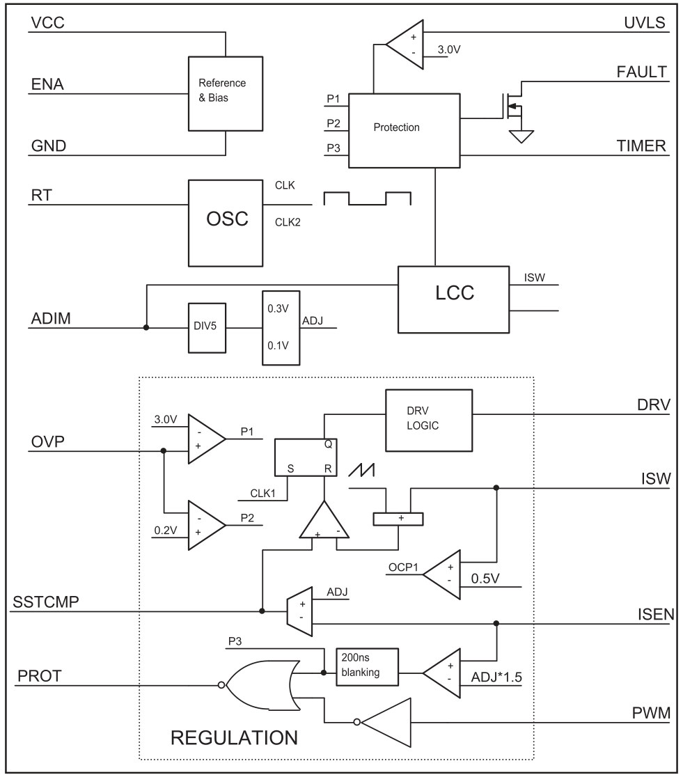
Fig. 6. OZ9902C block diagram
The OZ9902C is enabled by applying more than 2 V to the ENA input. Once the controller is on, the VREF output rises to 5.0 V (10 mA at VCC=12 V). Less than 1.0 V at ENA disables the controller.
If the VREF load exceeds 10 mA, overcurrent protection is triggered. When VREF drops below 3.6 V or the UVLS input drops below 2.9 V, the IC stops and enters lockout.
There is undervoltage lockout on the VCC pin with a 6.8 V threshold; the IC turns on when VCC rises above 7 V.
The controller runs at a fixed frequency set by the resistor at the RT pin (R610 in Fig. 5), which can be calculated as:
fOP [kHz]=6497/RRT [kΩ].
Here (RRT=R610=27 kΩ) the operating frequency is about 240 kHz.
The analog dimming range at the ADIM input is 0.5…1.5 V. The LED string current is set at the ISEN input, where the voltage can vary within 0.1…0.3 V. At VADIM=1.5 V the ISEN voltage is regulated at 0.3 V, and at VADIM=0.5 V at 0.1 V.
The LED string current can be calculated as:
ILED [mA]=VADIM [mV]/5×RISEN [Ω].
Here (RISEN=(R613 R614 R615 R637)=1 Ω) the current of the LED string connected to the driver output is ILED MIN=100 mA, ILED MAX=300 mA.
PWM dimming is controlled by an external signal at the DIM input in the 100 Hz…20 kHz range with levels above 2 V and below 1 V. A high level turns the LED string current on, a low level turns it off.
Overvoltage protection is triggered at more than 3 V at the OVP input. The converter shutdown delay is set by the timer: the TIMER output (pin 8) charges capacitor C611 (see Fig. 5) with 3 µA. If the voltage across C611 exceeds 3 V, switching stops and the IC latches off; it must be restarted via the ENA input. If the voltage across C611 does not reach 3 V and the OVP voltage falls below 3 V, the driver keeps running.
A short circuit at the converter output is detected when the OVP voltage is below 0.2 V; the IC latches off and restarts when VOVP rises above 0.2 V.
If the LED string return is shorted to ground through the high-voltage converter output, MOSFET Q602 is turned off immediately and C116 starts charging from the TIMER output at 3 µA. During this period the IC briefly turns Q602 on to check whether the short in the LED string is still present. If the short is removed before C116 reaches 3 V, the LED driver resumes operation; otherwise the IC shuts down and latches.
The current through converter MOSFET Q601 is monitored at the ISW input (pin 12); the voltage is taken from current sense resistors R625-R628 in the MOSFET source. If the ISW voltage exceeds 0.5 V, the MOSFET is turned off until the next switching cycle.
If during operation the ISEN voltage falls below 75 % of the level set by ADIM, output overcurrent protection is triggered and the IC shuts down after the delay set by the TIMER output (see above).
In normal operation the FAULT output is low. If any of the protections described above is triggered, the FAULT output goes high (open drain).
Parameters of the LED driver power components:
- Q601 MDD9N40 (N-MOSFET, VD=400 V, ID=6 A, RDS(ON)=0.85 Ω);
- D601 PDU540 (VR=400 V, IO=5 A, tRR=35 ns);
- Q602 MDD7N25 (N-MOSFET, VD=250 V, ID=6.5 A, RDS(ON)=0.55 Ω).
Typical power supply faults
The PSU does not start, mains fuse F1 blows
Inspect all components and PCB traces for burn marks, damage, cracked or swollen electrolytic capacitors (especially CE1, CE2). Replace all faulty parts. After replacement, check the PSU input (contacts L and N of connector P1) for a short circuit with an ohmmeter. If there is a short, to localize the faulty stage quickly, break the connection between the mains rectifier output and the PFC and DC/DC converter (point Z10 or VBUS in Fig. 2) and check these stages for shorts with an ohmmeter. In the faulty stage, check all active power components first.
In the rectifier stage, diodes BD1-BD4 and filter capacitors CE1, CE2 often fail; check the capacitors with an ESR meter even if they look fine.
In the PFC and converter stages, power MOSFETs QW1, QW2, diode D301 and snubber components D304, D305, R319, C303 usually fail. A failed MOSFET often damages controller U301 as well, so after replacing the transistors, before powering the PSU again, check the IC supply circuit and its gate driver outputs for shorts.
After power-on, the 12 V and 115 V outputs appear briefly and then disappear
To localize the faulty section, disconnect the PSU from the load (unplug connector P2), load the 12 V output with, for example, a 12 V/5…10 W car bulb, and simulate the P_ON signal by applying 5 V from an external source through a 10 kΩ resistor to pin 10 of P2. If the PSU now starts and the output voltages are present, the problem (assuming the main board is OK) is in the LED driver, which needs to be diagnosed (see below).
If nothing changes, the TEA1755 controller does not start. Fig. 7 shows the start conditions of the PFC and converter control blocks inside the controller.
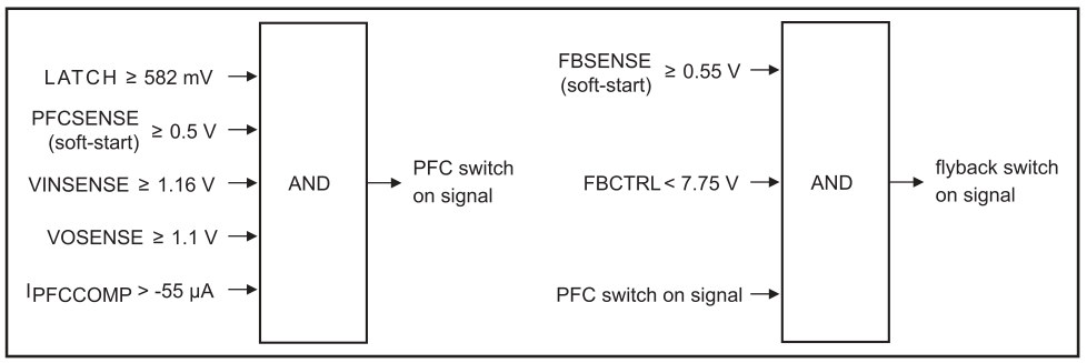
Fig. 7. Start conditions of the PFC and converter control blocks in TEA1755
Check that these conditions are met (see the description and Table 1), find and eliminate the cause.
The external output overvoltage protection circuit (U404, D401, D405, D406, Q402, PC2) may also be tripping. Check its operation (see the description above) and determine whether it is working correctly.
The PSU starts, 115 V and 12 V are present, but the 3.3 V standby voltage is missing
Connect the TV to the mains and check for 12 V at pins 3, 4 of connector P3 (Fig. 2) and for the 3.3 V output at pins 9-12 of P3. If 3.3 V is missing, check (replace) the standby power module.
The TV does not switch from standby to on, the standby LED is lit
At power-on, the P_ON signal at pin 10 of P2 must change from low to high (above 2.5 V). This signal controls MOSFET switch U405, which feeds 12 V to the TV main board. 12 V must appear at pins 7, 8 of U405. If it is zero, replace the IC.
The LED driver does not work — no LCD backlight (sound is present, no picture)
Check the LED driver control signals at PSU connector P2:
- BL_ON at pin 12 (backlight on, active high);
- P_DIM at pin 11 (PWM dimming signal).
If these signals are present along with 115 V (at L601, see Fig. 5) and 12 V (at pin 2 of U601) but there is no backlight, check the LED driver circuit (see the description above).
References
- NXP Semiconductors. TEA1755T. HV start-up DCM/QR flyback controller with integrated DCM/QR PFC controller. Rev. 1 — 25 October 2012. Product data sheet.
- NXP Semiconductors. AN11142. GreenChip TEA1755 integrated PFC and flyback controller. Rev. 2 — 13 September 2017.
- O2Micro. One Channel High Power LED Driver OZ9902C. 03/22/2010.
Source: Remont & Service magazine
Comments (0)
No comments yet. Ask a question about this circuit — we usually reply within a few days.