Electronics News
Archive : 18 December 2014 год
 Industry body NMI and the Electronic Systems Community (ESCO) have been given the opportunity to develop a new model for apprenticeships and are looking for industry support to define the scheme and get it off the ground.
According to the partners: "We are acutely aware of the shortage of engineering skills and are proactive at addressing opportunities. The UK Electronics Skills Foundation has already taken significant steps to improve the situation and we now have opportunity to open another new pathway to entering the ranks of professional electronic engineering."
The two organisations have been granted approval from the Department for Business, Innovation and Skills (BIS) to submit an Electronic Systems Trailblazer Apprenticeship proposal. "We believe the priority is to source high calibrate graduate engineers and therefore aim to submit a Level 6 (Graduate Engineer) Trailblazer," say the partners.
"We plan to build on models already in existence in our sector, where apprentices are employed after they complete A-Levels and continue their employment until they complete their degree."
Trailblazers are currently in receipt of up to £28,800 from BIS
NMI and ESCO are looking to create at least one generic job title and are considering:
• embedded electronic systems hardware engineer
• embedded electronics systems software engineer
• power electronics engineer.
The partners need to make a formal submission for the new Trailblazer by 15 February 2015 and want to hear from employers interested in defining the new standard and who can commit to taking at least one apprentice under the scheme from September 2015.
Author
Graham Pitcher
Source: www.newelectronics.co.uk
 In a development that holds promise for future magnetic memory and logic devices, researchers in the US have successfully used an electric field to reverse the magnetisation direction in a multiferroic spintronic device at room temperature.
The demonstration, made by a team from the US Department of Energy's Berkeley Lab, could lead to smaller, faster and cheaper ways of storing and processing data.
"Our work shows that 180° magnetisation switching in the multiferroic bismuth ferrite can be achieved at room temperature with an external electric field when the kinetics of the switching involves a two step process," said lead researcher Ramamoorthy Ramesh. "We exploited this multi step switching process to demonstrate energy efficient control of a spintronic device."
Multiferroics are materials in which unique combinations of electric and magnetic properties can simultaneously co-exist. They are viewed as potential cornerstones in future data storage and processing devices because their magnetism can be controlled by an electric field rather than an electric current, a distinct advantage as Heron explains.
"The electrical currents that today's memory and logic devices rely on to generate a magnetic field are the primary source of power consumption and heating in these devices," explained Ramesh. "This has triggered significant interest in multiferroics for their potential to reduce energy consumption while also adding functionality to devices."
Ramesh and his collaborators began by setting up a theoretical study in which an out-of-plane electric field was applied to bismuth ferrite films. They discovered a two-step switching process that relies on ferroelectric polarisation and the rotation of the oxygen octahedral.
"The two step switching process is key as it allows the octahedral rotation to couple to the polarization," said Ramesh. "The oxygen octahedral rotation is also critical because it is the mechanism responsible for the ferromagnetism in bismuth ferrite. Rotation of the oxygen octahedral also allows us to couple bismuth ferrite to a good ferromagnet such as cobalt-iron for use in a spintronic device."
To demonstrate the potential technological applicability of their technique, the researchers used heterostructures of bismuth ferrite and cobalt iron to fabricate a spin valve, a spintronic device consisting of a non-magnetic material sandwiched between two ferromagnets whose electrical resistance can be readily changed.
X-ray magnetic circular dichroism photoemission electron microscopy images confirmed a clear correlation between magnetisation switching and the switching from high to low electrical resistance in the spin valve.
"We also demonstrated that using an out-of-plane electric field to control the spin valve consumed energy at a rate of about one order of magnitude lower than switching the device using a spin polarised current," Ramesh concluded.
Author
Laura Hopperton
Source: www.newelectronics.co.uk
 Resistive RAM pioneer Crossbar says it has developed a method which suppresses the sneak path current; an effect which makes it difficult to read data reliably from individual memory cells. Without this ability, the company says, RRAM developers cannot deliver high density 3D memory arrays.
The company came out of 'stealth mode' earlier in 2014, when it disclosed its technology, in which one transistor is capable of driving more than 2000 interconnected memory cells. However, reading one particular cell is a challenge because of what's called the sneak path current. While current flows through the cell you're trying to read, it also flows through nearby cells, making it difficult to interpret the data. It also increases power consumption.
Crossbar says it has solved the problem using a super linear threshold layer. Here, a volatile conduction path formed at the threshold voltage creates a 'no leakage' region for unselected memory cells.
Sylvain Dubois, the company's VP of marketing and business development, said: "The challenge with RRAM has been how to read data and the way you look at a cell is critical.
"RRAM data is written by applying a voltage, but read by measuring current. Our solution creates a 'quiet zone' that allows the data in each cell to be read with confidence."
The difference in the on and off currents is said to be as great as 1010, whilst a turn on slope of less than 5mV/dec sees data recovered in less than 50ns.
According to Dubois, these features are additive when it comes to comparing the benefits of RRAM with flash. "RRAM's time to first data is about 1µs, where flash is about 100µs, so it's x100 better. But RRAM has a lower leakage current as feature size decreases, so the difference between the two approaches increases."
Now, Crossbar is transferring its technology to foundries. "The technology is CMOS compatible, so any CMOS foundry can produce memory," Dubois noted.
The company sees two main markets for RRAM technology. One is as embedded memory, where layers of RRAM cells can be manufactured on top of logic. The other is in high capacity storage, where it envisages devices capable of holding terabytes of data.
Author
Graham Pitcher
Source: www.newelectronics.co.uk
 An ultra low power RFID transponder chip that operates from a supply of less than 1V was described by Belgian research centre imec at the recent IEDM conference. The device, created using thin film transistor technology (TFTs) on plastic film, is said to pave the way for such applications as item level RFID tagging, body area networks and environmental monitoring.
The 8bit transponder chip, which can run from a 0.55V supply, consumes 2.5µW. At this level, says imec, a AAA battery could power the chip for more than 20 years. Because it is created on a 25µm foil, the device addresses such issues as cost and mechanical flexibility, thinness and robustness. It can also be embedded in security documents, smart packaging, disposable electronics or textiles.
The research has been done within the Holst Centre's industrial affiliation programme on thin film electronics, with support from the EU through the COSMIC project.
Pictured is a foil with plastic transponder chips developed by imec in 2010.
Author
Graham Pitcher
Source: www.newelectronics.co.uk
 According to certification specialist SGS, the phrase that manufacturers and importers should avoid, as part of a disclosure, is 'to the best of my knowledge'. It says this seemingly innocent statement is often used to cover up a lack of objective evidence or, in the worst case, is an attempt to cover up a known lack of compliance or the fact that a component or material contains a non conforming chemical.
SGS says the responsibility for compliance rests clearly with the brand owner and points out that if you accept 'to the best of my knowledge' or other such 'wiggle words' in a declaration, your company could be the subject of an EU RoHS Enforcement investigation, fines, recall of products, removal of CE Mark and significant damage to your brand image.
Its advice? Do not accept any declarations that contain this phrase or other such disclaimers. If a supplier is unable – or unwilling – to provide evidence of the substances contained in its supplied material, component or subassembly or proof that restricted substances are not present in its supplied items without the use of this phrase, how can it declare compliance?
The simple answer, says SGS, is that it can't and adds that, if you accept its declaration as proof of compliance as you build your product's Technical Documentation File, you will not be able to support the claim of compliance for your product.
Author
Graham Pitcher
Source: www.newelectronics.co.uk
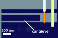 The atomic force microscope (AFM) is used by scientists to resolve features as small as individual atoms. Instead of magnifying with a lens, AFMs use a flexible cantilever with a tiny tip to 'feel' the surface. As a nanoscale feature is passed, interactions between the atoms on the tip and on the object's surface cause the cantilever to bend, revealing the finest of details.
Scientists have increased AFM sensitivity by making the tip vibrate at a particular frequency as it passes over the surface and measuring how much the frequency changes. This is because frequency can be measured more precisely than many other parameters.
However, calibrating the tip is an issue. Because AFMs operate in a near vacuum at temperatures approaching absolute zero, the tip and the specimen interact in a tight space behind several walls. In order to calibrate the tip, it has to be removed and checked at room temperature. This not only skews AFM results but also requires exotic calibration equipment.
Looking to sidestep such problems, scientists at the US National Institute of Standards and Technology (NIST) have developed a sensor that promises to increase AFM accuracy.
"With our sensor," says NIST's Gordon Shaw, "the tools you need to calibrate the tip are built right into the sensor, so it would not need to be removed from the AFM."
The sensor is a redesign of the device that makes the tip vibrate. Made of a silicate material, the cantilever is roughly 3mm long, with a mirror at the end that reflects light from an LED. The LED delivers a specific amount of energy and when the photons strike the mirror, they exert enough pressure to set the cantilever vibrating. The distance the tip travels upwards and downwards is said to be the critical figure needed to equate a change in the tip's frequency to a change in atomic force.
"The sensor is capable of resolving forces as small as femto Newtons," said Shaw. "It gives us a useful reference, which is hard to come by when you're working with such tiny forces."
Author
Graham Pitcher
Source: www.newelectronics.co.uk