Electronics News
Archive : 29 February 2016 год
Researchers from EPFL have developed conductive tracks that they say are almost as flexible as rubber and can be stretched up to four times their original length and in all directions. The team claims the electronics can also be stretched a million times without cracking or interrupting their conductivity.
Both solid and flexible, the researchers say this metallic and partially liquid film could be used to make circuits that can be twisted and stretched - for applications such as artificial skin on prosthetics or robotic machines. It could also be integrated into fabric and used in connected clothing. And because it follows the shape and movements of the human body, it could be used for sensors designed to monitor particular biological functions.
Owing to the high surface tension of some of these liquid metals, experiments conducted so far have produced relatively thick structures. "Using the deposition and structuring methods that we developed, it's possible to make tracks that are very narrow - several hundredths of a nanometre thick - and very reliable," explained Stéphanie Lacour, who runs the Laboratory for Soft Bioelectronic Interfaces (LSBI).
Apart from their unique fabrication technique, the researchers' secret lies in the choice of ingredients, an alloy of gold and gallium. Hadrien Michaud, a PhD student at LSBI, said: “The two materials are intertwined and they form a continuous film that maintains its conductivity even when the material is stretch to four times its length.”
Arthur Hirsch, another PhD student at LSBI added: "Not only does gallium possess good electrical properties, but it also has a low melting point, around 30°C, and, thanks to the process known as supercooling, it remains liquid at room temperature." The layer of gold ensures the gallium remains homogeneous, preventing it from separating into droplets when it comes into contact with the polymer, which would ruin its conductivity.
Author
Tom Austin-Morgan
Source: www.newelectronics.co.uk
 Researchers from Aston University are claiming that a laser-based technique first proposed in the 1970s could be used to counter the internet 'capacity crunch' - a phrase which has attracted much attention and is building presence as we want better, faster Internet and pervasive, instant connectivity to the global network.
To keep optical communications technology, which carries 99% of global data traffic, ahead of the projected growth in demand for bandwidth, researchers have turned their attention to tackling nonlinear distortions of signals travelling in fibre cables which is claimed to be the main cause for the continued expansion of data transmission rates. The researchers used a technique called ‘optical phase conjugation’ (OPC) to reduce the undesirable effect of nonlinearities in a high-capacity transmission link. The result was a 60% increase in the distance which information could travel and still be successfully received.
OPC is a method in optics to undo distortions in optical waves introduced by the medium in which they travel. It has been known for several decades but until now it had not been tested in optical communication systems with data rates on the order of Tbyte/s, which are expected for the next generation of communications technology. In this study the researchers used a single OPC device in a 2000km fibre link to show for the first time, in systems with data rates from 800Gbytes/s to 4Tbytes/s, that OPC can successfully deal with nonlinearities, improving signal quality and allowing information to travel further.
The main drawback of OPC is that it requires a symmetry in the transmission link which is said to be hard to achieve. This symmetry is needed because an OPC device manipulates optical signals in a way which allows them to “erase” distortions and noise accumulated in the first half of the link as they travel through the second. “This is identical to Netwon’s prisms, where the first of two identical prisms spreads white light out into a rainbow, and the second inverted prism collects the colours back together again. However, since we don’t yet know how to build an ‘inverted fibre’ we need to use a special ‘mirror’, the optical phase conjugator, to perform this trick,” explained Professor Andrew Ellis, who led the experiment.
Current commercial optical communications systems use amplifiers at regular intervals to boost the signal as it travels through the fibre. As they amplify the signal they break the symmetry in a transmission link crucial for OPC to operate effectively. However, as optical amplification technology improves and new types of components like Raman amplifiers enter the market, it is expected that the symmetry challenge will be largely resolved.
Prof Ellis added: “Some product development is clearly needed, but we are now really only waiting for the market demand to catch up with the technology, which it will within a couple of product cycles.”
Author
Tom Austin-Morgan
Source: www.newelectronics.co.uk
 Researchers at McGill University in Montreal believe it may be possible to construct a supercomputer based on adenosine triphosphate (ATP) – a substance that provides power to human cells. The team also believes that such a device could be smaller and more power efficient than current supercomputers.
The research team has created a chip measuring 1.5 cm square in which channels have been etched. Instead of electrons propelled by electrical charge, short strings of proteins – biological agents – travel around the circuit in a controlled way, with their movements powered by ATP. Because it is run by biological agents, the model bio-supercomputer the team has developed uses far less energy than standard electronic supercomputers.
“We’ve managed to create a very complex network in a very small area,” said Professor Dan Nicolau Sr, who began working on the idea more than a decade ago. “This started as a back of an envelope idea, with drawings of what looked like small worms exploring mazes.”
Although the model bio supercomputer could tackle a complex classical mathematical problem efficiently, the researchers recognise there is a lot of work required to move from a model to a full scale functional computer.
“Now this model exists as a way of successfully dealing with a single problem, there are going to be many others who will follow up and try to push it further, using different biological agents, for example,” said Prof Nicolau. “It’s hard to say how soon it will be before we see a full scale bio supercomputer. One option for dealing with larger and more complex problems may be to combine our device with a conventional computer to form a hybrid device. Right nowk, we're working on a variety of ways to push the research further.”
Pic: Till Korten
Author
Graham Pitcher
Source: www.newelectronics.co.uk
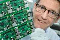 RS Components and element14 have unveiled the Raspberry Pi 3 Model B. The latest version of the credit card sized computer features an SoC based on a 64bit ARM Cortex A53 quad core processor, as well as integrated Bluetooth and wireless LAN connectivity IoT development projects.
Eben Upton, CEO of Raspberry Pi Trading, said: “Four years ago today, we launched the first Raspberry Pi. Today, we’re launching Raspberry Pi 3. It’s still $35 and it’s still the size of your credit card, but now it comes with on-board wireless LAN and Bluetooth, 50% more processing power, and a quad core 64bit processor. The new Raspberry Pi opens up even more possibilities for IoT and embedded projects; we hope you like it as much as we do.”
The board is based on the Broadcom BCM2837 SoC, which includes an ARM Cortex-A53 quad core processor running at 1.2GHz. A BCM43438 combo device provides IEEE802.11b/g/n wireless LAN, Bluetooth Classic and Bluetooth Low Energy connectivity. The BCM2837 also integrates a dual core VideoCore IV multimedia coprocessor.
“Raspberry Pi has taken another important step in its evolution,” said Lindsley Ruth, CEO of RS’ parent Electrocomponents. “Based on the robust and well proven combination of hardware and software of the Raspberry Pi platform, this latest generation board delivers even more processing power together with embedded wireless connectivity, plus software to make it easy for businesses or individuals to develop applications for the Internet of Things.”
Claire Doyle, global head of Raspberry Pi at element14, added: “Today, as we celebrate the fourth birthday of Raspberry Pi, we reach another major milestone on the Pi journey, with the launch of a faster, technically advanced board.
“Supported by our growing accessory portfolio, Raspberry Pi 3 allows customers to develop specific applications and build new projects – and we can’t wait to see what customers will do with it!”
Gordon Hollingworth, director of engineering at Raspberry Pi, noted some changes to the board. “Because the board’s form factor is fixed, there was only one place for the Wi-Fi antenna, which means the LED has moved. We’ve also launched a stronger Pi case, as well as an uprated power supply, because of the A53 processor.
“There is also a new compute module board – the CM3 – which will allow people to design their own board and to drop in the Pi module. The idea of this is for people to develop their system on a Pi, then move to the compute module to speed manufacturing.”
However, the module – which will not enter production for another six months – doesn’t feature Wi-Fi. “If we put it on the module,” Hollingworth said, “that would need certification and, to justify that, we would need to see volume.”
Author
Graham Pitcher
Source: www.newelectronics.co.uk
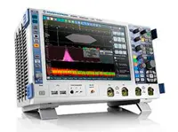 Said to be the most compact lab oscilloscope available for multidomain applications, the RTO2000 from Rohde & Schwarz allows complex measurements to be made quickly.
According to the company, the device allows developers to analyse how functional units in advanced embedded designs – such as power supplies, the processor system and the sensor technology – interact. The scope also displays correlations between time, frequency, protocol and logic analysis measurement results.
The RTO2000 is said to be the first oscilloscope in its class to offer a memory of up to 2Gsample. This supports the history function, which provides access to previously acquired waveforms, with a trigger timestamp allows time correlation. Users can view saved signals and analyse them using tools such as zoom, measurement, math and spectrum analysis functions.
New features are said to include peak list, maximum hold detectors and a logarithmic display, while a zone trigger enables the graphical separation of events in the time and frequency domains. Up to eight zones of any shape can be defined and the trigger is activated when a signal either intersects or does not intersect the zone.
Capable of capturing up to 1million waveform/s, the RTO2000 has a vertical resolution to up to 16bit, while HD mode enables configurable lowpass filtering of the signal after the A/D converter. In this way, says the company, users can trigger on the smallest signals.
The RTO2000 is available in two and four channel versions and with bandwidths of 600MHz, 1GHz, 2GHz, 3GHz and 4GHz.
Author
Graham Pitcher
Source: www.newelectronics.co.uk
 Researchers at MIT have demonstrated what they claim are the thinnest, lightest solar cells ever produced. This proof-of-concept shows an approach to making solar cells that could help power the next generation of portable electronic devices.
According to the researchers, the key to their approach is to make the solar cell, the substrate that supports it, and a protective overcoating to shield it from the environment, all in one process. The substrate is made in place and never needs to be handled, cleaned, or removed from the vacuum during fabrication, minimising exposure to dust or other contaminants that could degrade the cell’s performance.
Professor Vladimir Bulovic, MIT’s associate dean for innovation, said: “The innovative step is the realisation that you can grow the substrate at the same time as you grow the device.”
In this experiment, the team used a common flexible polymer called parylene as both the substrate and the overcoating, and an organic material called DBP as the primary light-absorbing layer. The entire process takes place in a vacuum chamber at room temperature and without the use of any solvents, unlike conventional solar-cell manufacturing, which requires high temperatures and harsh chemicals. In this case, both the substrate and the solar cell are ‘grown’ using established vapour deposition techniques.
To demonstrate just how thin and lightweight the cells are, the researchers placed a working cell on a soap bubble without popping the bubble. The researchers acknowledge that this cell may be too thin to be practical, but parylene films of thicknesses of up to 80µm can be deposited using commercial equipment, without losing the other benefits of in-line substrate formation.
While the solar cell in this demonstration device is not especially efficient, because of its low weight, its power-to-weight ratio is claimed to be among the highest ever achieved. This is significant for applications where weight is important, such as on spacecraft or on high-altitude helium balloons used for research. Whereas a typical silicon-based solar module, whose weight is dominated by a glass cover, may produce about 15W of power per kilogram of weight, the MIT team says its cells have demonstrated an output of 6W per gram - around 400 times higher.
“It could be so light that you don’t even know it’s there, on your shirt or on your notebook,” said Prof Bulovic. “These cells could simply be an add-on to existing structures.”
The team says that developing these cells into a manufacturable product will take time. Yet while commercial success in the short term may be uncertain, this work could open up new applications for solar power in the long term.
Pic: To demonstrate just how thin and lightweight the cells are, the researchers draped a working cell on top of a soap bubble, without popping the bubble.
Author
Tom Austin-Morgan
Source: www.newelectronics.co.uk
 The desire to gather more information about manufacturing equipment embodied in Industry 4.0 is pushing sensor manufacturers to make smaller, but more capable devices which generate less heat.
Looking to help them meet these challenges, Maxim Integrated has launched the MAX14827, a dual channel 250mA IO-Link transceiver which is said to integrate the high voltage functions commonly found in industrial sensors, including two low power drivers with active reverse polarity protection to reduce downtime. It also includes 3.3V and 5V linear regulators for low noise analogue/logic supply rails.
The third generation device, specified at Maxim’s Munich facility, is intended to provide manufacturers with flexibility. Reinhardt Wagner, senior corporate applications engineer, said: “There are many types of sensor and different levels of complexity. For example, it could be an intelligent device or a simple binary switch. Our intent was to develop a flexible chip to meet these needs.”
Sensors that work in association with an MCU can use the SPI interface, while IO-Link operation is supported by a three wire UART interface. A multiplexed UART/SPI option allows a serial MCU interface to be shared by the SPI and UART interfaces.
A typical on-resistance of 2.5? is said to cut power dissipation by half, while the 2.5 x 2.5mm chip scale package saves space. Specified for temperatures ranging from -40 to 125°C, the part is also available in a 4 x 4mm TQFN.
Author
Graham Pitcher
Source: www.newelectronics.co.uk
 Building on its expertise in developing RF transceivers for medical applications, Microsemi has unveiled a low power sub GHz transceiver for industrial systems. According to the company, the ZL70550 brings ‘best in class’ low power characteristics, a high level of integration and an extremely small footprint.
Francois Pelletier, product line director, said the company’s medical devices had been developed to use the MICS band, which spans 402 to 405MHz. “Devices using this band can’t be used for anything but implantable technology, so we’ve developed a chip for industrial applications with the same features.”
Operating in ISM bands ranging from 779 to 965MHz and with a range of up to 200m, the ZL70550 consumes 2.8mA while transmitting at -10dBm and consumes 2.5 mA during reception. A sleep current of 10nA is said to suit it to low duty cycle applications.
The ZL70550 operates from a supply ranging from 1.7 to 3.6V and supports variable output power and data rates up to 200kbit/s. For those applications requiring extended range, output power, input sensitivity and data rate can be adjusted to give a link budget up to -107dBm.
“By leveraging the same intellectual property,” Pelletier added, “we have successfully developed for implantable pacemakers and hearing aids where power consumption cannot be compromised, we are able to provide the lowest power wireless link in a small form factor that is easy to deploy.”
The ZL70550 is available in a 3 x 2 mm chip scale package or in 5 x 5mm QFN. Microsemi notes that, other than an antenna and, in some cases, its matching network, only a crystal, resistor and two coupling capacitors are required.
Author
Graham Pitcher
Source: www.newelectronics.co.uk
 A collaboration organised by the Industrial Internet Consortium (IIC) and involving Bosch Rexroth, Cisco, Intel, KUKA, National Instruments, Schneider Electric and TTTech is developing the first Time Sensitive Networking (TSN) testbed.
“Testbeds are a major focus and activity of the IIC and its members,” said IIC executive director Dr Richard Soley. “Our testbeds are where the innovation and opportunities of the industrial Internet – new technologies, new applications, new products, new services and new processes – can be initiated, thought through and rigorously tested to ascertain their usefulness and viability before coming to market.”
The testbed, which will be hosted by NI, will:
- Combine different critical control traffic (such as OPC UA) and best effort traffic flows on a single, resilient network based on IEEE 802.1 TSN standards
- Demonstrate TSN’s real time capability and vendor interoperability using standard converged Ethernet
- Assess the security value of TSN and provide feedback on the ability to secure initial TSN functions
- Show ability for the IIoT to incorporate high-performance and latency-sensitive applications
Speaking exclusively to New Electronics, Rahman Jamal, NI’s global technology and marketing director, said: “NI is now involved in four IIC test beds: track and trace; microgrids; condition monitoring; and, now, TSN.
“The TSN test bed is all about applications in the manufacturing environment with different types of device. It’s the first test bed to be based on TSN.”
The collaboration aims to produce a reference architecture for manufacturing environments and to produce results within the next six months or so, according to Jamal.
Ralf Koeppe, vice president of engineering and manufacturing, electric drives and controls, Bosch Rexroth, added: “We regard the TSN testbed to be a very important contribution for further improvement of vendor interoperability and of exchanging data in an IIoT infrastructure.”
Author
Graham Pitcher
Source: www.newelectronics.co.uk
 A research group from Cornell University in the US believes its work with quantum dot solids might help to usher in a new era in electronics.
The team, led by associate professor Tobias Hanrath, has fused together lead-selenium nanocrystal building blocks to form atomically coherent square superlattices.
The difference between these and previous crystalline structures is the atomic coherence of each 5nm crystal. Because the crystals are connected to each other, their electrical properties are, potentially, superior to those of existing semiconductor nanocrystals. Potential applications are said to include energy absorption and light emission.
The strong coupling of the nanocrystals leads to formation of energy bands that can be manipulated, based on the crystals’ makeup, and could be the first step toward discovering and developing other artificial materials with controllable electronic structures.
In 2013, Hanrath’s group reported an approach to connecting quantum dots through the controlled displacement of a connector molecule. That paper said ‘connecting the dots’ was one of the hurdles to be overcome. But it notes that barrier seems to have been cleared with this new research.
Researcher Kevin Whitham said he sees the team’s work as a sort of challenge for other researchers. “This is as far as we know how to push it now,” he said. “But if someone were to come up with some technology, some chemistry, to provide another leap forward, this is challenging others to ask ‘how can we do this better?’.”
Hanrath said the discovery can be viewed in two ways. “It’s the equivalent of saying ‘now we’ve made a really large single crystal wafer of silicon and you can do good things with it’,” he said, referencing the early days of semiconductor technology. “That’s the good part. But the potentially bad part is … that if you wanted to improve on our results, those challenges are going to be really, really difficult.”
Pic: Kevin Whitham, Cornell University
Author
Graham Pitcher
Source: www.newelectronics.co.uk