Electronics News
Archive : 19 March 2016 год
 A team of researchers from the US Department of Energy’s Oak Ridge National Laboratory (ORNL) have developed a processing technique that could bring two-dimensional electronic devices closer to their ultimate promise of low power, high efficiency and mechanical flexibility.
Led by Olga Ovchinnikova of ORNL's Centre for Nanophase Materials Sciences Division, the team used a helium ion microscope on a layered ferroelectric surface of a bulk copper indium thiophosphate. This resulted in the discovery of a material with tailored properties potentially useful for mobile phones, photovoltaics, flexible electronics and screens.
Ovchinnikova said: "Our method opens pathways to direct-write and edit circuitry on 2D material without the complicated current state-of-the-art multi-step lithographic processes."
The team noted that while the helium ion microscope is typically used to cut and shape matter, they demonstrated that it can also be used to control ferroelectric domain distribution, enhance conductivity and grow nanostructures. Their work could establish a path to replace silicon as the choice for semiconductors in some applications.
Alex Belianinov, part of Ovchinnikova’s team, said: "Everyone is looking for the next material - the thing that will replace silicon for transistors. 2D devices stand out as having low power consumption and being easier and less expensive to fabricate without requiring harsh chemicals that are potentially harmful to the environment."
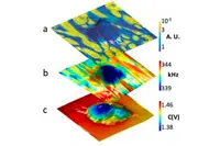
Pic: This diagram illustrates the effect of helium ions on the mechanical and electrical properties of the layered ferroelectric
Author
Tom Austin-Morgan
Source: www.newelectronics.co.uk
 Scientists from Moscow Institute of Physics and Technology (MIPT) and the Moscow State University claim to have developed a memory cell based on superconductors that could work hundreds of times faster than the types of memory devices currently used.
Alexander Golubov, head of MIPT's Laboratory of Quantum Topological Phenomena in Superconducting Systems, said: "With the operational function that we have proposed in these memory cells, there will be no need for time-consuming magnetisation and demagnetisation processes. This means that read and write operations will take only a few hundred picoseconds, depending on the materials and the geometry of the particular system, while conventional methods take hundreds or thousands of times longer than this."
Golubov and his colleagues have proposed creating basic memory cells based on quantum effects in ‘sandwiches’ – or Josephson junctions - comprised of a dielectric (or other insulating material) between two layers of superconducting material. The electrons are able to tunnel from one layer of a superconductor to another through the insulating layer.
Josephson junctions with ferromagnets used as the middle layer are currently said to be of greatest practical interest. In memory elements that are based on ferromagnets the information is encoded in the direction of the magnetic field vector in the ferromagnet. However, there are two fundamental flaws with this process: firstly, the low density of the ‘packaging’ of the memory elements - additional chains need to be added to provide extra charge for the cells when reading or writing data, and secondly the magnetisation vector cannot be changed quickly, which limits the writing speed.
The group of physicists from MIPT and MSU proposed encoding the data in Josephson cells in the value of the superconducting current. By studying the superconductor-normal metal/ferromagnet-superconductor-insulator-superconductor junctions, the scientists discovered that in certain longitudinal and transverse dimensions the layers of the system may have two energy minima, meaning they are in one of two different states. These two minima can be used to record data.
In order to switch the system from ‘zero’ to ‘one’ and back again, the scientists have suggested using injection currents flowing through one of the layers of the superconductor. They propose to read the status using the current that flows through the whole structure. These operations can be performed hundreds of times faster than measuring the magnetisation or magnetisation reversal of a ferromagnet.
Golubov added:"Our method requires only one ferromagnetic layer, which means that it can be adapted to so-called single flux quantum logic circuits, and this means that there will be no need to create an entirely new architecture for a processor. A computer based on single flux quantum logic can have a clock speed of hundreds of gigahertz, and its power consumption will be dozens of times lower."
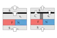
Pic: Superconducting currents during reading various states of the memory cell are shown. The greater current the larger the arrow.
Author
Tom Austin-Morgan
Source: www.newelectronics.co.uk
 The MEMS Design Contest has been launched by Cadence Design Systems, Coventor, X-FAB and Reutlingen University at DATE 2016. The contest aims to encourage greater ingenuity with regard to the integration of MEMS devices and mixed-signal CMOS blocks.
Design teams are encouraged to propose design concepts that combine MEMS and mixed-signal technologies. The organisers will provide free training workshops to familiarise the participating teams with the design tools, design methodologies and process technologies involved.
A panel of industry professionals and academics will undertake appraisal of the submissions. Each submission will be judged on the degree of innovation demonstrated in hardware and methodology, the novelty of the application and the value the design provides. Awards for the top three submissions will be presented at Cadence’s annual user conference, CDNLive EMEA 2018, in Munich and the winning team’s solution will be manufactured at X-FAB’s wafer production facilities.
“Supporting innovation and advancement in electronic design is fundamental to what this contest is all about,” said Alexander Duesener, corporate VP EMEA of Cadence Design Systems. “Creating mixed-signal logic and MEMS designs requires a new process flow and totally new thinking. By enabling the winning design team to turn their concepts into manufactured designs, we highlight the value of MEMS and mixed-signal designs in today’s products.”
Author
Tom Austin-Morgan
Source: www.newelectronics.co.uk
 IDTechEx Research has projected that the graphene market will grow to $220m in 2026. This forecast is at the material level and does not count the value of graphene-enabled products. According to the research, continual decline in average sales prices will accompany the revenue growth, meaning that volume sales will reach nearly 3800 tonnes per annum in 2026.
Despite this, forecasts by IDTechEx Research in the report ‘Graphene, 2D Materials and Carbon Nanotubes: Markets, Technologies and Opportunities 2016-2026’ suggest that the industry will remain in a state of over-capacity until 2021 beyond which time new capacity will need to be installed. Furthermore, the report forecasts that nearly 90% of the market value will go to graphene platelets, as opposed to sheets.
“The market will be segmented across many applications, reflecting the diverse properties of graphene,” said Dr Khasha Ghaffarzadeh, head of consulting, IDTechex. “In general, we expect functional inks and coatings to reach the market earlier. This is a trend that we forecasted several years ago and is now observed in prototypes and small-volume applications. Indeed, IDTechEx Research projects that the market for functional inks and coatings will make up 21% of the market by 2018.”
The applications for conductive inks are numerous: anti-corrosion coatings, transparent conducting electronics, glucose test strips, car seat headers, de-icers, etc. Graphene can be added to carbon inks to improve conductivity and branding, and can be added to zinc-based anti-corrosion coatings to reduce zinc loading. IDTechEx has forecast that this will be a $25m market in 2022 at the material supply level.
The research forecasts that the energy storage sector will control 25% of the market in 2026, with nearly $100m of graphene sold into it. Here too, graphene will play the role of an additive to improve the performance of carbon-based Li-ion electrodes. Silicon anode and lithium sulphur batteries also represent long term opportunities, with these devices forecast to become $4.3b and $1.2b markets in 2026, respectively.
However, the largest sector will be the composites sector, which will grow to nearly $60m in 2026 at the material supply level, controlling 40% of the market. Here, graphene additives are expected to be used for converting low-cost, low-performance plastics into low-cost, high-performance ones.
Author
Tom Austin-Morgan
Source: www.newelectronics.co.uk