Electronics News
Archive : 19 August 2017 год
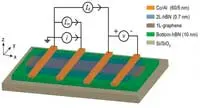 A device based on a bilayer of graphene and boron nitride which is said to show unprecedented spin transport efficiency at room temperature has been created by Graphene Flagship scientists based at the University of Groningen, The Netherlands.
According to the researchers, the spin signal is so large that it can be used in real life applications such as spin based logic gates and transistors.
The research team showed that they could greatly improve the efficiency of the injection and detection of spin electrons into graphene by using the insulator boron nitride in between the graphene layer and the ferromagnetic spin injector/detector electrodes.
“Graphene is a very good material for spin transport, but it does not allow one to manipulate the spins,” says Professor Bart van Wees. “To inject spins into the graphene, one has to make them pass from a ferromagnet through a boron nitride insulator by quantum tunnelling. We found that using a two-atom layer of boron nitride resulted in a very strong spin polarisation of up to 70% – ten times what we usually get.”
In the devices produced, the researchers claim the polarisation increased with voltage, challenging the current thinking that it is only the ferromagnetic that polarises spin. Instead it would seem that it is the quantum tunnelling that polarises the spin.
The researchers also found a similar tenfold increase in spin detection in the same device. “So overall, the signal increased by a factor of 100,” said van Wees.
“We can now inject spins into graphene and measure them easily after they travel some distance. One application would be as a detector for magnetic fields.”
Author
Peggy Lee
Source: www.newelectronics.co.uk
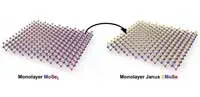 A semiconducting transition-metal dichalcogenide (TMD) has been created by Rice laboratory scientists from a monolayer of molybdenum diselenide from which the top layer of the lattice was stripped and replaced with sulphur.
The new material they call Janus sulphur molybdenum selenium (SMoSe) has a crystalline construction the researchers claim can host an intrinsic electric field and that also shows promise for catalytic production of hydrogen.
"This type of two-faced structure has long been predicted theoretically but very rarely realised," said materials scientist Jun Lou. "The break of symmetry in the out-of-plane direction of 2D TMDs could lead to many applications, such as a basal-plane active 2D catalyst, robust piezoelectricity-enabled sensors and actuators at the 2D limit."
The two-faced material is technically two-dimensional, but like molybdenum diselenide it consists of three stacked layers of atoms arranged in a grid.
According to the researchers, tight control of the conditions in a typical chemical vapor deposition furnace – 800°C at atmospheric pressure – allowed the sulphur to interact with only the top layer of selenium atoms and leave the bottom untouched.
The researchers claim the presence of sulphur gave the material a larger band gap than molybdenum diselenide.
Author
Peggy Lee
Source: www.newelectronics.co.uk