Electronics News
Archive : 28 October 2017 год
 Wide bandgap semiconductors, seen as significantly more energy-efficient, have emerged as leading contenders in the creation of FETs for next-generation power electronics.
While diamond is believed to be the most ideal wide band gap material, one of the challenges in creating diamond MOSFETs is increasing the hole channel carrier mobility. However, researchers from France, the UK and Japan believe they may have solved this problem using the deep-depletion regime of bulk-boron-doped diamond MOSFETs. The proof of concept enables simple diamond MOSFET structures to be produced from single boron-doped epilayer stacks. Using this approach, mobility is said to be increased by an order of magnitude.
According to the team, many of the diamond MOSFETs demonstrated to date have relied on a hydrogen-terminated diamond surface to transfer positively charged carriers – holes – into the channel. More recently, operation of oxygen terminated diamond MOS structures in an inversion regime, similar to the common mode of operation of silicon MOSFETS, has been demonstrated.
To build their MOSFET, the researchers deposited a layer of aluminum oxide at 380°C over an oxygen-terminated thick diamond epitaxial layer. Holes were created in the diamond layer by incorporating boron atoms into the layer; boron has one less valence electron than carbon, which acts like the addition of a hole. The bulk epilayer functioned as a thick conducting hole channel. The transistor was switched from the on- to the off-state by application of a voltage which repelled and depleted the holes – the deep depletion region. In silicon-based transistors, this voltage would have formed an inversion layer and the transistor would not have turned off.
“We fabricated a transistor in which the on-state is ensured by the bulk channel conduction through the boron-doped diamond epilayer,” said Julien Pernot, a researcher at the NEEL Institute in France. “The off-state is ensured by the thick insulating layer induced by the deep-depletion regime. Our proof of concept paves the way in fully exploiting the potential of diamond for MOSFET applications.”
The researchers plan to produce these structures through their new startup called DiamFab.
Collaborating in the project were researchers from Universite Grenoble Alpes, CNRS Institut NEEL, CNRS G2Elab, Université de Toulouse, University of Cambridge, University of Tsukuba and Institut Universitaire de France.
Author
Graham Pitcher
Source: www.newelectronics.co.uk
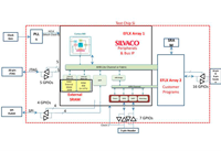 Flex Logic has demonstrated an initial version of what it calls a flexible microcontroller design. The approach, unveiled at ARM TechCon, integrates an embedded FPGA on MCU processor and peripheral buses. This, says the company, will enable ‘unprecedented improvements in performance, cost and time to market for next generation chips’.
“This announcement is a major milestone in the industry as it shows designers a complete implementation of embedded FPGA and provides a ‘breadboard’ for MCU and SoC architects to experiment with the architecture to develop their own products,” claimed Geoff Tate, Flex Logix’ CEO. “A flexible microcontroller has a block of embedded FPGA, with appropriate RAM resources, on the processor bus and can be configured and reconfigured by the customer to accelerate the workloads that matter in their applications. The embedded FPGA also can implement programmable I/O either directly or on the peripheral bus, enabling customers to implement the flavour of serial I/O they require and/or to do processing of I/O to offload the host processor.”
A flexible microcontroller with embedded FPGA is said to save mask costs, speed time to market and to enable customers to deploy their own accelerators.
The concept design is based on a Cortex-M0 core, with peripherals from Silvaco combined with a reconfigurable accelerator and reconfigurable I/O. It also features Flex Logix’ TSMC16FFC validation chip, which implements an EFLX200K array and ‘substantial’ RAM.
Jim Bruister, Silvaco’s director, digital systems, noted: “Our AMBA subsystems and peripherals are an excellent match for the EFLX array family and we look forward to working with Flex Logix’ customers to provide reconfigurable solutions.”
Author
Graham Pitcher
Source: www.newelectronics.co.uk
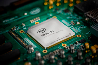 Intel has started shipping the Stratix 10 SX FPGA. The device, which integrates a quad-core ARM Cortex-A53 processor and features more than 1million logic elements, is said to suit 5G wireless communication, software defined radio, secure computing for military applications, network function virtualisation and data centre acceleration.
“With Intel Stratix 10 SX FPGAs, Intel reaffirms its ‘all in’ commitment to SoC FPGA devices,” said Reynette Au, vice president of marketing for Intel’s Programmable Solutions Group. “We now provide a wide set of options for customers needing processors and FPGAs, with device offerings across the low-end, mid-range and now, high-end FPGA families, to enable their system designs.”
Manufactured on Intel’s 14nm process technology, the Stratix10 SX combines the ARM hard processor system with the Intel HyperFlex core fabric architecture to create what it calls a high-performance and power-efficient SoC FPGA.
Designs can be created using the Intel SoC FPGA Embedded Development Suite , which also enables customers to access the ARM Development Studio 5 Intel SoC FPGA Edition to code, build, debug and optimise applications.
Author
Graham Pitcher
Source: www.newelectronics.co.uk
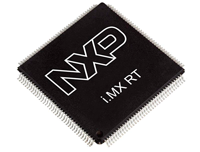 NXP says it is creating a new category called the crossover processor with the introduction of the RT1050, a device said to blend the benefits of applications processors with those of microcontrollers.
Geoff Lees, general manager of NXP’s microcontroller business, said the i.MX RT is intended for edge processing applications. “NXP sees this as relating to every connected device down to the MCU level. Everything will have some processing requirement, along with management, analytics, wireless connectivity and HMI support. And this device also has built in physical security.”
According to Lees, customers developing low cost applications have asked for a device which can support an RTOS running on a Cortex-A7 platform. “While we have done that,” Lees noted, “that carries a large overhead and the implementation is not as efficient as it could be.”
In the i.MX RT, the Cortex-A7 core is replaced by a Cortex-M7. “We use the M7 to increase real time performance,” Lees explained, “particularly latency. So we started with the i.MX6 UL, removed the A7 domain, along with the caches and so on, and dropped in an M7. The result is a device which is more optimised for real time applications. And we’ve gone from concept to production in less than 12 months.
“Running the M7 at high clock rates can bring power consumption penalties,” Lees continued, “but we are geared up to put the i.MX RT into production at 600MHz with 512kbyte of SRAM.”
At the moment, the part is targeted for production on an 40nm process and Lees claims the device will consume 100µA/MHz – up to three times less than comparable parts.
The first part in the range, the RT 1050, is sampling and will be in volume production shortly. “One thing we have focused on,” Lees continued, “is making sure real time response is in the nanosecond range – and the RT 1050 has a latency of about 20ns. We’ve also made sure that all SRAM on chip can be used either as tightly coupled memory or as general purpose RAM.”
As Lees noted, the RT 1050 resembles the i.MX6 UL. “We’ve retained the high performance communications features of the i.MX, but have added a number of peripherals to support MCU related tasks.” And he pointed out that, by removing the A7 core, enough die space was created to allow a DC/DC converter to be integrated on chip.
The BGA packaged device – which will sell for less than $3 – has been designed so that it can be used on a four layer PCB. “A typical i.MX needs six to eight layers,” Lees noted.
NXP will also be sampling a ‘cut down’ version of the chip at the end of 2017. The 1020 will come in a QFP with 256kbyte of SRAM, but Lees noted that some peripherals which don’t make sense for a QFP device will be omitted. “Wire bonding will also mean it has to run at 500MHz.”
More RT parts are in development. “While the 1050 comes with 512k of RAM, we’re working on parts with many times that,” Lees said, “as well as working on 28nm variants. Our target is 5Mbyte of RAM and that makes no sense on 40nm. Moving to 28nm will also halve the power consumption, so that’s significant.”
Further down the line, Lees expects MRAM to appear in the chips. “It’s good for economies of scale and it’s a back end process. Being able to take a standard design and overlay MRAM without impacting cost is very attractive. NXP recently presented a test chip with 8Mbit of MRAM,” he concluded. “It’s not near production, but watch this space.”
Author
Graham Pitcher
Source: www.newelectronics.co.uk
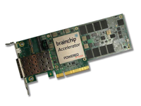 Artificial intelligence and machine learning specialist Brainchip says it has shipped a BrainChip Accelerator card to a major European automobile manufacturer.
Bob Beachler, senior vice president for marketing and business development, said: “This is an exciting first evaluation of BrainChip Accelerator. Our spiking neural network provides instantaneous ‘one-shot’ learning, is fast at detecting, extracting and tracking objects and is very low-power. These are critical attributes for automobile manufacturers processing the large amounts of video required for ADAS and AV applications.”
According to the company, the Accelerator increases the performance of object recognition provided by its software and algorithms. The low-power accelerator card can detect, extract and track objects using proprietary spiking neural network technology. It is said to provide a sevenfold improvement in images/second/Watt, compared to traditional convolutional neural networks accelerated by GPUs.
“We look forward to working with this world-class automobile manufacturer in applying our technology to meet its requirements,” Beachler added.
Author
Graham Pitcher
Source: www.newelectronics.co.uk