Electronics News
Archive : 12 February 2018 год
 Farnell element14 has launched the GraspIO Cloudio - a Raspberry Pi add-on board with a Drag and Drop programming interface on iPhone, iPad, Android.
Other features include: Voice Assistant Capabilities, IFTTT (“If This Then That”) Integration, IoT Cloud Service, Sensor Monitor and Dashboard, Custom Notifications with Image and Video and One Tap Multi-Board Upload.
“The GraspIO Cloudio, when combined with a Raspberry Pi, is a Full Stack IoT platform meaning that you can programme IoT devices simply and quickly with drag and drop programming on a mobile app,” explained Steve Carr, Global Head of Marketing at Premier Farnell and Farnell element14.
“The combination of built-in hardware facilities and access to application software will make Cloudio a valuable addition to the range of tools available to developers of projects involving voice, motion, imaging and cloud interaction.”
Cloudio unlocks physical computing applications with Raspberry Pi through a number of features that include: a 0.96-inch OLED display, IR sensor, light sensor, temperature sensor, tactile switch, three ADC ports, a mini servomotor port for external sensors, three digital output ports, an RGB LED, and a buzzer.
Potential applications for the Cloudio include: voice control, users can create their own voice assistants using the inbuilt speech recognition feature to control Cloudio from a smartphone; speech output in which projects can be made to “talk” with the easy-to-use in-application “Speak” block and the Raspberry Pi’s own headphone jack and, using Cloudio’s on-board or external sensors, it can be deployed as an edge device to design intelligent and responsive sensor monitoring projects. Real-time sensor graphs can be viewed on a mobile device and data can be exported for IoT analytics.
Author
Neil Tyler
Source: www.newelectronics.co.uk
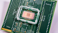 Imec, the research and innovation hub in nanoelectronics and digital technologies, has designed and fabricated a 16,384-electrode, 1,024-channel micro-electrode array (MEA) for high-throughput multi-modal cell interfacing.
The chip offers intracellular and extracellular recording, voltage- and current-controlled stimulation, impedance monitoring and spectroscopy functionalities. It has the most cell-interfacing modalities on a single chip and is the only one to enable multi-well assays.
According to imec the chip has created a platform that enables high quality data acquisition at increased throughput in cell-based cell studies.
MEAs have long been used for in vitro cell-interaction experiments but most MEAs do not support high throughput measurements, making current cell-assays time-consuming. Typically passive devices, without built-in circuitry, they require complex external equipment for data acquisition. In addition, most MEAs are not able to accommodate the extra sensing modalities to fully characterise complex cell behaviour and interactions.
Imec’s CMOS-MEA has been able to pack 16,384 active electrodes with signal processing, filtering and analogue-to-digital conversion on-chip, resulting in a compact system with easy interfacing. Each electrode has a miniature pre-amplifier to improve the signal quality.
The electrodes are grouped in 16 clusters, each of which can be addressed individually, making it possible to run 16 experiments independently and simultaneously.
This CMOS-MEA also includes 1,024 low-noise readout channels that can be connected to any of the 16,384 electrodes. The custom reconfigurable on-chip circuits support 6 cell-interfacing modalities: both extra- and intracellular electrical activity recording, constant voltage and constant current stimulation for cell excitation or localized electroporation, fast impedance monitoring and, finally, impedance spectroscopy.
While fast impedance monitoring can detect impedance changes over time and cell presence for optimal electrode selection, single-cell impedance spectroscopy gives detailed information of the electrode impedance, seal resistance and cell-membrane impedance which can be used for cell differentiation.
Imec’s high input impedance, low noise and low power reconfigurable circuits make it possible to integrate 1,024 parallel readout channels and 64 reconfigurable stimulation units on a small chip area.
“Not only are we reporting the highest number of modalities so far on a single chip with a very high channel count, we are able to achieve this without any performance penalty. Moreover, by offering six modalities on such large scale, the imec CMOS-MEA will greatly improve the throughput and versatility of cell-based assays,” commented Nick Van Helleputte, manager biomedical circuits at imec. “With the introduction of CMOS chip technology into the MEA-technology, we have realized a breakthrough in cell interfacing.”
Imec’s micro-electrode array chip will be presented at ISSCC in San Francisco.
Author
Neil Tyler
Source: www.newelectronics.co.uk
 Your body may be the new way to portably charge wearable devices.
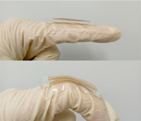
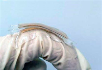
In a collaborative project, the University at Buffalo (UB) and Institute of Semiconductors at Chinese Academy of Science (CAS) are working together to devise a metallic tab, known as the triboelectric nanogenerator.
The most common form of triboelectric charging is static electricity and the research team has proposed numerous nanogenerators that they believe will utilise this effect.
The idea is that the tab (1.5 centimeters long, by 1 centimeter wide) will attach to the body and generate electricity from small movements such as, bending a finger, which will be delivered to a user’s wearable device.
"No one likes being tethered to a power outlet or lugging around a portable charger. The human body is an abundant source of energy.” says lead author Qiaoqiang Gan. “We thought, why not harness it to produce our own power?”
The challenge is that most nanogenerators that work with triboelectrics are difficult to manufacture or expensive. However, the team claims that the tab they’re developing address both these issues.
The device is said to comprise two thin layers of gold, with polydimethylsiloxane (PDMS) sandwich between. One of the layers of gold is stretched, which according to the team is vital to the operation. This is because it will cause it to crumple upon release and when force is reapplied, for example from a small body movement, the motion creates friction between the gold layers and PDMS.
"This causes electrons to flow back and forth between the gold layers. The more friction, the greater the amount of power is produced," explains another lead author, professor Yun Xu, at CAS.
The researchers say the tab will be capable of delivering a maximum voltage of 124V, a maximum current of 10 microamps and a maximum power density of 0.22 millwatts per square centimeter.
This is currently not quick enough to charge a smartphone, but the researchers say that in their experiments, it did light 48 red LED lights.
Nan Zhang, a PhD student at UB has been tasked with improving this performance. Zhang’s team plan on using larger pieces of gold, which they hope when stretched and folded together will generate more electricity.
The researchers are also working towards a portable battery to store energy produced by the tab, in a hope to one day power wearables and self-powered electronic devices.
Pic: Prototype of the triboelectric nanogenerator
Author
Bethan Grylls
Source: www.newelectronics.co.uk
 A research team led by the University of Buffalo believes electronic devices could be powered by a small metallic tab that would generate electricity through the bending a finger or by other simple movements.
“No one likes being tethered to a power outlet or lugging around a portable charger,” said lead researcher Qiaoqiang Gan. “The human body is an abundant source of energy, so why not harness it to produce our own power?”
The tab is a triboelectric nanogenerator. While a number of nanogenerators that use the triboelectric effect have been proposed, most are said to be difficult to manufacture or to not be cost effective. The tab developed by the University of Buffalo team is said to address both of those concerns.
The device comprises two thin layers of gold, with a layer of polydimethylsiloxane (PDMS) sandwiched in between. When a finger is bent, for example, the motion leads to friction between the gold layers and PDMS.
“This causes electrons to flow back and forth between the gold layers,” said Professor Yun Xu from research partner the Chinese Academy of Sciences. “The more friction, the greater the amount of power produced.”
According to the team, a tab measuring 1.5 x 1cm delivered a maximum of 124V, a maximum current of 10µA and a maximum power density of 0.22mW/cm2. This, the researchers assert, was enough to light 48 red LED lights simultaneously.
University of Buffalo undergraduates have been tasked with improving the tab’s performance, including the use of larger pieces of gold to deliver more electricity.
Researchers are also developing a portable battery to store energy produced by the tab and envision the system serving as a power source for various wearable and self-powered electronic devices.
Author
Graham Pitcher
Source: www.newelectronics.co.uk
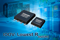 Toshiba Electronics Europe is shipping two new 100V additions to its low-voltage U-MOS IX-H N-channel power MOSFET series, designed for power supply applications in industrial equipment and motor control applications.
The devices are fabricated with Toshiba’s latest low-voltage U-MOS IX-H trench process, which it says optimises the element structure. According to Toshiba, the TPH3R70APL and TPN1200APL also deliver the industry’s lowest-in-class on-resistance of 3.7mΩ and 11.5mΩ respectively.
The devices are said to exhibit low output charge (QOSS: 74 / 24nC) and low gate switch charge (QSW: 21 / 7.5nC) and allow for a 4.5V logic level drive.
Compared with current devices that the U-MOS VIII-H process, Toshiba claims these devices have lower key figures of merit for MOSFETs for switching applications including RDS(ON) Qoss, and RDS(ON) QSW.
The TPH3R70APL is housed in a 5mm x 6mm SOP advance package and are said to be capable of handling drain currents (ID) up to 90A, while the TPN1200APL is in a 3mm x 3mm TSON advance package and handles ID levels up to 40A.
Author
Bethan Grylls
Source: www.newelectronics.co.uk