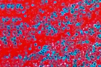
 Continuing the recent trend for researchers to develop novel 2D materials, a team from the Lawrence Berkeley National Laboratory (LBNL) in the US has successfully grown 2D sheets of organic-inorganic hybrid perovskites from solution. The sheets, said to be large and square shaped, exhibited photoluminescence, colour tunability and what is called a ‘unique structural relaxation’ not found in covalent semiconductor sheets.
“We believe this is the first example of 2D atomically thin nanostructures made from ionic materials,” says Peidong Yang, a chemist with LBNL’s Materials Sciences Division. “The results of our study open up opportunities for fundamental research on the synthesis and characterisation of atomically thin 2D hybrid perovskites and introduces a new family of 2D solution processed semiconductors for nanoscale optoelectronic devices, such as field effect transistors and photodetectors.”
Traditional perovskites are typically metal-oxide materials that display a range of electromagnetic properties. Recently, organic-inorganic hybrid perovskites have been solution-processed into thin films or bulk crystals which have enabled photovoltaic devices to reach power conversion efficiencies of 20%.
According to the team, a preliminary photoluminescence study indicates a band edge emission at 453nm. This is said to suggest that colour tuning could be achieved by changing the thickness of the sheets, as well as the composition.
The geometry of these square shaped 2D crystals is said to imply high quality crystallinity and their large size is likely to facilitate their integration into future devices. “With our technique, vertical and lateral heterostructures can also be achieved,” Yang concluded. “This opens up new possibilities for the design of materials/devices on an atomic/molecular scale with distinctive new properties.”
Author
Graham Pitcher
Source: www.newelectronics.co.uk
