Electronics News
Archive : 27 January 2015 год
 "OM tools and mitigation practices are also becoming increasingly sophisticated and, as a result, we believe there is a real need for a professional body capable of providing best-practice guidance, training, career development and qualifications to an emerging class of professional obsolescence managers."
Electronic component obsolescence has always presented numerous design challenges for engineers, who have to address issues such as continuity, quality, cost management and support for the total life of the product. It is no longer simply about the component.
"It's a critical design challenge," says Blackman, "but one that has often been overlooked. Collaboration between end product manufacturers, original component manufacturers, component distributors and project consultants is crucial. We believe that obsolescence management is something that shouldn't be outsourced; organisations need to be able to manage it in-house."
A growing number of companies and organisations have been looking to undertake formal training in obsolescence management but have been unable, until now, to provide any meaningful record of the training being undertaken or to offer recognised industry-backed qualifications, explains Blackman.
As a result, the IIOM – supported by the University of Maryland in the US and by the Cranfield University and the Ministry of Defence – is working to introduce tiered membership classes, which will allow individuals from any country to progress along a defined career path in Obsolescence Management.
"These classes will range from Student membership, with no competence requirements, up to classes which will require members to prove their competency by completing an IIOM-approved course and passing a final examination," explained Blackman. "These classes of membership will entitle qualifying individuals to use post nominal letters – Associate (AIIOM), Member (MIIOM) and Fellow (FIIOM)."
In order to ensure that training standards are met, the IIOM will also establish an international network of IIOM Endorsed Trainers and Assessors.
"Trainers will focus on developing the OM skills of individual members, while Endorsed Assessors will audit projects and organisations for compliance against the International Obsolescence Management Standard IEC 62402:2007," Blackman continued.
According to Blackman courses in obsolescence will be available in April 2016.
IIOM is also planning to host a biennial International Conference. The first of these will take place in Edinburgh in June 2015.
Author
Neil Tyler
Source: www.newelectronics.co.uk
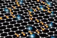 A team of researchers from three US universities has demonstrated a way to vary the number of electrons in a give region of a piece of graphene. The team says this is a proof of principle in the creation of semiconductor devices using the so called 'wonder material'. It adds that the number of electrons can be tuned through the application of an electric field and says this could enable future devices to be 'rewired' dynamically.
The research has been conducted at the University of Pennsylvania, the University of California, Berkeley and the University of Illinois at Urbana-Champaign.
"We've come up with a non destructive, reversible way of doping that doesn't involve any physical changes to the graphene," said Andrew Rappe from the University of Pennsylvania.
The technique involves depositing a layer of graphene so it rests on, but doesn't bond to, a layer of lithium niobate. Lithium niobate is ferroelectric, meaning that it is polar, and its surfaces have either a positive or negative charge. Applying an electric field pulse can change the sign of the surface charges.
The researchers took advantage of the fact that a certain type of the material, periodically poled lithium niobate, is manufactured so that it has 'stripes' of polar regions that alternate between positive and negative.
"Because the lithium niobate domains can dictate the properties," said Moonsub Shim from the University of Illinois, "different regions of graphene can take on different character, depending on the nature of the domain underneath. That allows a simple means of creating a p-n junction or even an array of p-n junctions on a single flake of graphene. Such an ability should facilitate advances in graphene that might be analogous to what p-n junctions and complementary circuitry has done for the current state-of-the-art semiconductor electronics."
Because the oxide polarisation can be altered, the type and extent of supported graphene doping can also be altered. Lane Martin from UC Berkeley said: "You write an 'up' domain or a 'down' domain in the region you want and the graphene's charge density would reflect that change. You could make the graphene over that region p-type or n-type, and, if you change your mind, you can erase it and start again."
This is said to represent an advantage over chemically doped semiconductors because once atomic impurities are added, they can't be removed. Future research will investigate the feasibility of designing dynamic semiconducting devices with this technique.
Author
Graham Pitcher
Source: www.newelectronics.co.uk
 Renesas Electronics says the RX71M group – the flagship product in the RX Family of 32bit microcontrollers – is now shipping. Developed for use in industrial equipment, the devices run at up to 240MHz and come with up to 4Mbyte of on chip flash.
The RX71M group features 112 variants, pin counts ranging from 100 to 177 pins, flash capacities from 2 to 4Mbyte and 512kbyte of RAM.
The RX700 series operates at up to 240MHz, double the previous maximum operating frequency. This is said to equate to 4.4CoreMarks/MHz at 240MHz, which Renesas says is amongst the best performing flash MCUs. The RXv2 core is said to deliver 1.3 times the performance of the earlier RXv1 core, whilst maintaining code compatibility.
Manufactured on a 40nm process and capable of operating at 120 MHz, and the advanced fetch unit (AFU) incorporating exclusive cache-based memory control technology, achieve performance equivalent to no-wait access when operating at 240 MHz. Even if a cache miss occurs, the performance penalty is equivalent to only one cycle, so excellent real-time performance can be achieved even when using only the flash memory.
The parts, available in a choice of TFLGA, LFBGA and LQFP packages, operate from a supply in the range from 2.7 to 3.6V.
Author
Graham Pitcher
Source: www.newelectronics.co.uk
 Ofcom has announced plans that it says will ensure the UK plays a leading role in developing the Internet of Things. As part of its plan, Ofcom wants to create a regulatory environment which fosters investment and innovation in the IoT sector.
According to Ofcom, there are already more than 40million devices connected via the IoT in the UK; a figures forecast to grow by more than eight times by 2022.
Acting chief executive Steve Unger, pictured, said: "The IoT will bring benefits to a range of sectors and could change the way we live our lives. As a result of this growth, we have listened closely to industry and want to develop a framework for this technology to evolve in a way which will ultimately benefit citizens and consumers."
Ofcom's plan is to ensure the UK has the tools and infrastructure to allow the IoT to develop unhindered. The plans require Ofcom to work closely with government, other regulators and industry to remove any unnecessary barriers to the IoT's development, while building a regulatory environment which fosters innovation and ensures issues, such as data protection, are addressed.
The regulator has identified four areas, following consultations in 2014.
Spectrum availability: Ofcom's analysis has shown that, whilst much of the IoT's short to medium term spectrum demands are met with current initiatives, it will need to continue to monitor the IoT's spectrum requirements to help identify when additional spectrum may be needed.
Data privacy: Whilst much data is protected by legislation such as the Data Protection Act 1998, Ofcom will work with the Information Commissioner's Office, government, other regulators and industry to explore solutions to data privacy issues.
Network security and resilience: Ofcom will investigate how its existing activities on security and resilience of the UK's communications networks can include the IoT.
Network addressing: Ofcom will continue to monitor the progress being made by internet service providers in supporting IPv6 connectivity.
Author
Graham Pitcher
Source: www.newelectronics.co.uk
![]() Fujitsu has started mass production of gallium nitride (GaN) power devices for switching applications at its 150mm fab in Fukushima. The move follows the announcement in 2013 that it was integrating its GaN business with that of Transphorm.
Fujitsu has started mass production of gallium nitride (GaN) power devices for switching applications at its 150mm fab in Fukushima. The move follows the announcement in 2013 that it was integrating its GaN business with that of Transphorm.
"The start of mass production in a CMOS compatible fab is a significant step forward toward achieving the widespread use of GaN power devices, as well as a demonstration of the successful integration of both companies' strengths," said Haruki Okada, president of Fujitsu Semiconductor. "We will continue to enhance our high quality manufacturing technology to support the stable supply of the products and bring the new value of GaN power devices to the world."
The automotive qualified Fukushima facility will allow dramatic expansion of Transphorm's GaN power device business. "Manufacturing Transphorm's GaN power devices at the Fujitsu facility will assure our customers of a scalable, stable supply of products with the stamp of Fujitsu's proven, high quality standard in mass manufacturing," said Transphorm CEO Fumihide Esaka. "We will continue to expand our GaN power device portfolio with continued partnership with Fujitsu."
Author
Graham Pitcher
Source: www.newelectronics.co.uk
 A Kevlar based barrier between the electrodes in a lithium-ion battery has been developed by the University of Michigan. The development is believed to prevent fires of the kind believed to have grounded Boeing's 787 Dreamliner in 2013.
The barrier is said to stifle the growth of metal tendrils that can become unwanted pathways for electrical current. "Unlike other ultra strong materials, such as carbon nanotubes, Kevlar is an insulator," said Professor Nicholas Kotov. "This property is perfect for separators that need to prevent shorting between two electrodes."
Lithium-ion batteries work by moving lithium ions from one electrode to the other. This creates a charge imbalance and, since electrons cannot pass through a membrane between the electrodes, they go through a circuit instead.
If the holes in the membrane are too big, lithium atoms can create dendrites, similar to the copper dendrite pictured. These can pass through the membrane and if they reach the other electrode, the electrons have a path within the battery. The pores in the Kevlar based membrane are 15 to 20µm in diameter; small enough to block the tips of the dendrites.
Author
Graham Pitcher
Source: www.newelectronics.co.uk
 Engineers from Università degli Studi di Pavia have created a micro-ring that entangles individual particles of light. The design is based on a micro ring resonator, a loop etched onto a silicon wafer that can capture and emit particles of light. By tailoring the resonator's design, the researchers created a small and highly efficient source of entangled photons.
"The main advantage of our new source is that it is small, bright and silicon based," said researcher Daniele Bajoni. "The diameter of the ring resonator is 20µm. Previous sources were hundreds of times larger than the one we have developed.
"In the last few years, silicon integrated devices have been developed to filter and route light, mainly for telecommunication applications," he continued. "Our micro-ring resonator can be readily used alongside these devices, moving us toward the ability to fully harness entanglement on a chip."
The research could find application in quantum information technologies –and quantum cryptography protocols in particular. According to Bajoni and his colleagues, these protocols have been demonstrated and tested, but what has been missing was a cheap, small, and reliable source of entangled photons capable of propagation in fibre networks.
Author
Graham Pitcher
Source: www.newelectronics.co.uk
 A recent discovery by a team at École polytechnique fédérale de Lausanne (EPFL) in Switzerland suggests that it is possible to create conductive pathways several atoms wide in a material, move them around at will and make them disappear.
The approach – called adaptable electronics – is generating interest because of the many applications, including one chip performing the tasks of several different circuits. As an example, says the research team, a circuit assigned to process sound information could, when not being used for this purpose, be reassigned to process images. This, it adds, would allow electronic devices to be miniaturised.
A further benefit of the approach could be resilient circuits: if a chip is damaged, it could theoretically reconfigure itself using the components that remain intact.
Underpinning the work are ferroelectric materials, in which flexible conductive pathways can be generated by applying an electric field. When the current is applied, certain atoms move 'up' or 'down' – or polarisation. Recently, it has been seen that conductive pathways several atoms wide –'walls' – form between these polarised zones, but it has not been possible to control how these pathways form.
The EPFL researchers have shown the formation of walls on a film of ferroelectric material sandwiched between platinum components can be controlled and pathways created at given sites. "By applying electric fields locally on the metal part," said researcher Leo McGilly, "we were able to create pathways at different sites and move them. We couls also destroy them with a reverse electric field."
The research team has tested its work on isolated materials, but the next will be to develop a prototype reconfigurable circuit. McGilly concluded: "The fact that we can generate pathways wherever we want could allow us to imitate in the future phenomena that take place inside the brain, with the regular creation of new synapses. This could prove useful in reproducing the phenomenon of learning in an artificial brain."
Author
Graham Pitcher
Source: www.newelectronics.co.uk
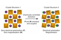 Scientists at the University of Liverpool have controlled the structure of a material to simultaneously generate both magnetisation and electrical polarisation. The team says the development has potential applications in information storage and processing.
Making a single material demonstrating magnetisation and electrical polarisation is said to be difficult because the electronic requirements for obtaining them in a material are typically contradictory: characteristics which favour polarisation often disfavour magnetisation. However, the researchers, from the University's School of Physical Sciences, showed that by making designed changes to a structure, it is possible to create these properties in a material – a perovskite, in this case – which initially displayed neither.
Professor Matthew Rosseinsky said: "We were able to demonstrate that magnetisation and polarisation are coupled by measuring the linear magnetoelectric coefficient, a key physical quantity for the integration of such materials in a device. This coupling arises because both properties are produced by the same single set atomic motions that we built in to the material.
"There are a number of challenges still to address, particularly switching the polarisation and making the material more electrically insulating, before applications of this material for information storage can be considered."
Author
Graham Pitcher
Source: www.newelectronics.co.uk
 PragmatIC Printing, a leading flexible electronics company, has completed a £5.4million funding round led by Cambridge Innovation Capital (CIC) with support from ARM Holdings and existing shareholders.
Scott White, chief executive officer, said: " We have become accustomed to silicon chips being incorporated into high value documents such as passports and credit cards , but there are limitations to how robustly and cost-effectively this can be done. Our technology platform creates a microcircuit that can be easily embedded in any flexible surface."
PragmatIC, headquartered in Cambridge and with a production facility based at the National Centre for Printable Electronics in Sedgefield, will use the funding to hire more staff and to scale up its production capacity to 100million flexible circuits. The funding will also allow PragmatIC to broaden its circuit design activities, to include applications such as sensors, processors and wireless communications.
Victor Christou, senior investment director of CIC, said: "PragmatIC's flexible electronics offers the most compelling and cost effective product I've seen in the 20 years I've been involved in this industry. The company has already demonstrated a scalable and cost effective manufacturing process. With CIC's support, the company can now meet the pent up demand from customers for higher volume commercial production."
"ARM is committed to identifying innovative and disruptive new technology platforms," said Mike Muller, ARM's chief technology officer. "We are supporting PragmatIC as it has the potential to dramatically extend the range of form factors and economics of embedded intelligence."
White added: " We are hugely excited by both the additional resources and the strategic contribution that will result from this investment by CIC and ARM. We look forward to further developing our technology platform and blue chip customer base through the course of 2015."
Author
Graham Pitcher
Source: www.newelectronics.co.uk