Electronics News
Archive : 30 October 2015 год
 Integrated Device Technology (IDT) has introduced a hardware and software solution that is claimed to simplify IEEE 1588 synchronisation of network communications equipment. The 82P339xx-1 products are composed of IEEE 1588-compliant software and IDT Synchronisation Management Unit (SMU) chips that deliver a complete telecom network synchronisation solution for IEEE 1588 and synchronous Ethernet.
Network synchronisation based on IEEE 1588 Telecom Boundary Clocks (T-BC) is said to be a practical and cost-effective alternative to deploying Global Navigation Satellite System (GNSS) antennas at every node in the network.IEEE 1588 Telecom Boundary Clocks compliant with ITU-T G.8273.2 enable the recovery of accurate frequency and phase/time information over a packet-based network.
The IDT T-BC hardware is claimed to be deterministic, simpler and more automated than alternative silicon solutions as it requires less external processor intervention. The hardware/software solution includes an IEEE 1588 protocol stack, clock recovery servos for frequency and phase/time, and clock synthesis hardware with physical layer frequency support.
“Packet-based synchronisation has historically been challenging for system designers to implement because it requires a broad range of specialised technology and needs to meet stringent network standards,” said Louise Gaulin, vice president and general manager of IDT’s Network Communications Division. “The 82P339xx-1 products were specifically engineered to be easy to use, flexible and to comply with the latest generation of packet-based synchronisation standards.”
The 82P339xx-1 SMUs are said to automatically filter IEEE 1588 phase/time information and combine it with physical layer frequency information in accordance with ITU-T G.8273.2 to generate accurate, stable and low-jitter clocks. The phase/time and frequency filters are implemented in hardware to ensure deterministic filter bandwidths, eliminating the need for additional software processing.
The 82P339xx-1 series is designed for applications including base stations, access equipment, routers, switches, optical equipment and servers.
Author
Tom Austin-Morgan
Source: www.newelectronics.co.uk
 Belgian nanotechnology research centre imec, along with Ghent University, has created arrays of indium phosphide lasers integrated monolithically on 300mm silicon substrates in a CMOS pilot line. The achievement is said to provide a path toward high volume manufacturing of cost effective photonic integrated circuits with monolithically integrated laser sources. The approach could help to speed data transfer between future logic and memory chips.
Widespread adoption of silicon photonics has been hampered, says imec, by the lack of monolithically integrated laser sources. One reason is the large mismatch in crystal lattice constants between both materials. The partners say they have overcome these structural differences and ‘largely suppressed’ the crystal defects that typically form at the interface between silicon and InP.
Using a production grade metal organic vapour phase epitaxial growth reactor, the partners were able to grow InP selectively on silicon in a pre patterned oxide template. This allowed InP waveguide arrays to be formed across the whole of the 300mm substrate. Grating structures etched in the top layer of these waveguides provide the optical feedback required for laser operation.
Typical lasing threshold powers of around 20mW were observed at room temperature under optical pumping, with small variability along the array. In addition, say the partners, accurate control on the distribution of lasing wavelengths in the array was demonstrated by modifying the grating parameters.
Author
Graham Pitcher
Source: www.newelectronics.co.uk
 Researchers from the National University of Singapore (NUS) have developed a hybrid magnetic sensor that they claim is more sensitive than most commercially available sensors. This could encourage the development of smaller and cheaper sensors for fields such as consumer electronics, information and communication technology and automotive.
When an external magnetic field is applied to certain materials, a change in electrical resistance, also known as magnetoresistance, occurs as the electrons are deflected. The discovery of magnetoresistance paved the way for magnetic field sensors used in hard disk drives and other devices, revolutionising how data is stored and read.
In the search for an ideal magnetoresistance sensor, researchers have prized the properties of high sensitivity to low and high magnetic fields, tunability, and very small resistance variations due to temperature.
The hybrid sensor developed by the team, led by Associate Professor Yang Hyunsoo of the Department of Electrical and Computer Engineering at NUS’ Faculty of Engineering, may finally meet these requirements.
The sensor, made of graphene and boron nitride, includes layers of carrier-moving channels, each of which can be controlled by the magnetic field.The researchers characterised the sensor by testing it at various temperatures, angles of magnetic field, and with a different pairing material.
Dr Kalon Gopinadhan, of the NUS Nanoscience and Nanotechnology Institute and the Centre for Advanced 2D Materials, said: “We started by trying to understand how graphene responds under the magnetic field. We found that a bilayer structure of graphene and boron nitride displays an extremely large response with magnetic fields. This combination can be utilised for magnetic field sensing applications.”
Compared to other existing sensors, which are commonly made of silicon and indium antimonide, the group’s hybrid sensor displayed higher sensitivity to magnetic fields. In particular, when measured at 127°C, the researchers observed a gain in sensitivity of more than eight-fold over previously reported laboratory results and more than 200 times that of most commercially available sensors.
Another breakthrough in this research was the discovery that mobility of the graphene multilayers can be partially adjusted by tuning the voltage across the sensor, enabling the sensor’s characteristics to be optimised. In addition, the sensor showed very little temperature dependence over room temperature to 127°C range.
Graphene-based magnetoresistance sensors hold immense promise over existing sensors due to their stable performance over temperature variation, eliminating the necessity for expensive wafers or temperature correction circuitry. Production cost for graphene is also much lower than silicon and indium antimonide.
Potential applications for the new sensor include the automotive industry, where sensors in cars, located in devices like flow meters, position sensors and interlocks, are currently made of silicon or indium antimonide. For instance, when there is a change in temperature due to the car’s air-conditioner or heat from the sun, properties of the conventional sensors in the car change as well. To counter this, a temperature correction mechanism is required, incurring additional production cost. However, with the team’s new hybrid sensor, the need for expensive wafers to manufacture the sensors, and additional temperature correction circuitries can be eliminated.
Assoc Prof Yang said: “Our sensor is perfectly poised to pose a serious challenge in the magnetoresistance market by filling the performance gaps of existing sensors, and finding applications as thermal switches, hard drives and magnetic field sensors.”
Following this proof-of-concept study, the researchers plan to scale up their studies and manufacture industry-size wafers for industrial use.
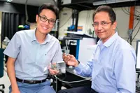
Pic: Associate Professor Yang Hyunsoo and Professor Thirumalai Venkatesan, Director of NUS Nanoscience and Nanotechnology Institute
Author
Tom Austin-Morgan
Source: www.newelectronics.co.uk
 Researchers at Cambridge University have developed a working laboratory demonstrator of what they call the ‘ultimate battery’. The lithium-oxygen battery is said to have high energy density, to be more than 90% efficient and which has, so far, been recharged more than 2000 times.
The energy density of the battery is said to be comparable to that of gasoline, which would allow a car to drive from London to Edinburgh on one charge.
According to the team, lithium-oxygen batteries have been viewed as the ‘ultimate’ battery due to a theoretical energy density ten times that lithium-ion battery.
The demonstrator relies on a highly porous – or ‘fluffy’ – carbon electrode made from graphene (comprising one-atom-thick sheets of carbon atoms) and additives that alter the chemical reactions in the battery, making it more stable and more efficient.
“What we’ve achieved is a significant advance for this technology and suggests whole new areas for research – we haven’t solved all the problems inherent to this chemistry, but our results do show routes forward towards a practical device,” said Professor Clare Grey of Cambridge’s Department of Chemistry.
By engineering the structure of the electrode, adding lithium iodide and changing the chemical makeup of the electrolyte, the researchers reduced the ‘voltage gap’ between charge and discharge to 0.2V, equating to an energy efficiency of 93%.
Additionally, the demonstrator can only be cycled in pure oxygen, the , nitrogen and moisture in air are generally harmful to the metal electrode.
While the results, reported in the Science, are promising, the researchers caution that a practical lithium-air battery remains at least a decade away.
Author
Graham Pitcher
Source: www.newelectronics.co.uk
 Ambiq Micro has announced that its Apollo microcontroller (MCU) has been selected by Misfit as the ‘brain’ in the Misfit Shine 2 Fitness and Sleep Monitor.
The next-generation Misfit Shine 2 is claimed to provide new features, functions and capabilities without sacrificing its six month battery life.Shine 2 tracks activity and sleep with a three-axis accelerometer and newly added three-axis magnetometer, displays progress, tells time, and gets users motivated with Misfit Move, a feature that encourages users to be active with a vibrational nudge.
"Shine 2 would not be what it is without this processor,” said Steve Diamond, VP of Hardware Engineering at Misfit. "It allowed us to focus less on power optimisation and more building a next-generation product with the same great battery life."
The Apollo MCU will operate as the central processor and controller in the new Misfit Shine 2, handling overall device operations including processing inputs from the device’s motion and environmental sensors and also controlling wireless communication with the outside world.
Ambiq Micro’s interim CEO, Mike Noonen, said: “The Ambiq Micro team is thrilled that our order of magnitude low power advantage is used so effectively in the Shine 2.”
Based on the 32-bit ARM Cortex-M4 with FPU, in real-world applications the Apollo MCU delivers typically 5 to 10 times lower energy consumption than other competitive MCUs. This high level of performance per watt can mean significantly extended battery life, the use of smaller or fewer batteries, and/or the ability to add new features not previously possible.
The reduction in energy consumption is achieved using Ambiq’s Subthreshold Power Optimised Technology platform. The Apollo MCU consumes 34µA/MHz when executing instructions from flash memory and features sleep-mode currents as low as 140nA.
Author
Tom Austin-Morgan
Source: www.newelectronics.co.uk
 Element14 has signed an exclusive global agreement with Raspberry Pi Trading to provide design and manufacturing services to OEM customers looking to create bespoke designs using the Raspberry Pi technology platform.
In what was described as the next phase in the development of the Raspberry Pi Eben Upton, CEO of Raspberry Pi Trading, said, “We are expecting to produce 3miilion boards this year and this deal will enable our customers to customise the Raspberry Pi for a particular design.
“Around 1million Raspberry Pi’s are already being used in industrial or embedded applications and this announcement comes in response to customer requests. We believe it will enable OEMs and, more importantly, SMEs to produce industrial grade products while avoiding the need for the large volumes usually associated with cost efficiencies.”
According to Richard Curtin, senior director, strategic alliance, at element14,“We will be able to support OEMs through every step of the design process from concept right through to the manufacture of the final boards.
“Customers from the engineering and maker markets will have access to over 200 engineers through our in-house technology businesses AVD and Embest Technologies.
“This agreement opens up the opportunity for customers to customise the Raspberry Pi technology platform to better suit specific applications across a wide range of industries – from the Internet of Things to industrial and end customer devices. We think we will be able to address the needs of a large number of verticals.”
According to element14 the ability to reconfigure the board layout will enable designers to add additional functionality, redesign interfaces allowing the board to connect to other equipment and change the board and memory configuration.
“As these will be bespoke designs it is envisaged that order quantities will start in the region of between 3-5,000,” Curtin said, “but it will depend on the nature of the customisation required.”
Reaction to the announcement has generally been positive although some concerns have been expressed at the minimum order level, which may put the service beyond the reach of smaller businesses.
The announcement also comes after Intel recently announced the release of the Arduino 101 - a stripped-back computer that is likely to go on sale next year.
Author
Neil Tyler
Source: www.newelectronics.co.uk