Electronics News
Archive : 30 January 2016 год
 Xilinx has announced the first shipment of the Virtex UltraScale+ FPGA, claimed to be the industry’s first high-end FinFET FPGA built using TSMC’s 16FF+ process.
Victor Peng, executive vice president and general manager of the Programmable Products Group at Xilinx, said: “The successful delivery of our Virtex UltraScale+ FPGA marks the availability of all three UltraScale+ 16nm families, which are already providing more than one hundred customers with the ability to develop next generation designs using cutting edge FinFET-based devices, development boards and tools. Our “Three-Peat” execution – with three consecutive generations of leadership technology at 28nm, 20nm, and now at 16nm – showcases our sustained commitment to being first to market with the most advanced products in our industry.”
Virtex UltraScale+ devices are said to build on the Virtex UltraScale family, the industry’s only 20nm high-end FPGAs. With capabilities like 32G transceivers, PCIe Gen 4 integrated cores, and UltraRAM on-chip memory technology, the new devices provide the required performance and integration needed for data centres, 400G and Terabit Wired Communications, Test and Measurement, and Aerospace and Defence markets.
Author
Tom Austin-Morgan
Source: www.newelectronics.co.uk
 AVnu Alliance has announced that Rockwell Automation and Kollmorgen have joined its industrial segment. The two companies are said to bring valuable expertise to AVnu Alliance activities incorporating standards such as Time Sensitive Networking (TSN) into a common networking foundation.
Industrial automation and information company, Rockwell has a history of technological innovation in industrial control systems.
Joe Kann, vice president, Global Business Development, Rockwell Automation, said: "We continue to evolve our industrial control and information solutions to help customers drive real-time productivity and innovation as they strive towards building a Connected Enterprise. By participating in the AVnu Alliance, we plan to share our industry knowledge and work together with other members towards further enhancing standard IP-based Ethernet for manufacturing."
Kollmorgen, a supplier of motion control solutions has demonstrated a commitment to open communication standards and network flexibility.
Steve Crass, VP North America Industrial Automation and Aerospace & Defence at Kollmorgen, commented: "Kollmorgen's business as a provider of innovative high-speed motion solutions is driven by ever-evolving customer needs for high-performance, multi-device fieldbus options. Joining AVnu provides us with a forum that will support open systems architectures for many years to come."
The addition of these companies demonstrates the importance of the continued evolution of standard Ethernet through TSN. The experience with control networking that these companies possess is expected to complement the existing efforts within the AVnu Alliance to define a common foundation for the Industrial Internet. This next step for standard Ethernet will enable complete convergence of standard IT traffic and the control system and will enable IoT for the industrial, automation and manufacturing sectors.
Gary Stuebing, AVnu Alliance president, said: "The AVnu Alliance looks forward to their contributions and forward-thinking philosophies when it comes to automation and how it can improve a variety of industrial processes."
Author
Tom Austin-Morgan
Source: www.newelectronics.co.uk
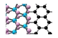 Researchers from MIT have reported the first chip-fabrication technique that they claim could enable significantly different materials to be deposited in the same layer. They also report that, using the technique, they have built chips with working versions of all the circuit components necessary to produce a general-purpose computer.
The layers of material in the researchers’ experimental chip measure between one and three atoms thick. This work could aid efforts to manufacture thin, flexible, transparent computing devices, which could be laminated onto other materials. “The methodology is universal for many kinds of structures,” said Xi Ling, form the MIT’s Research Laboratory of Electronics. “This offers us tremendous potential with numerous candidate materials for ultrathin circuit design.”
Previously, only materials with closely matched lattices have been deposited laterally in the same layer of a chip. The researchers’ experimental chip however, uses molybdenum disulphide and graphene, two materials with different lattice sizes.
To assemble their laterally integrated circuits, the researchers first deposit a layer of graphene on a silicon substrate. Then they etch it away in the regions where they wish to deposit the molybdenum disulfide. Next, at one end of the substrate, they place a solid bar of a material known as PTAS.
They heat the PTAS and flow a gas across it and across the substrate. The gas carries PTAS molecules with it that stick to the exposed silicon but not to the graphene. Wherever the PTAS molecules stick, they catalyse a reaction with another gas that causes a layer of molybdenum disulfide to form.
The technique also has implications for the development of the ultralow-power, high-speed computing devices known as tunnelling transistors and, potentially, for the integration of optical components into computer chips.
Because electron tunnelling is immune to the thermal phenomena that limit the efficiency of conventional transistors, tunnelling transistors can operate at very low power and could achieve much higher speeds.
Author
Tom Austin-Morgan
Source: www.newelectronics.co.uk
 Researchers at the University of Valencia (UV) are developing an ultra-low threshold semiconductor laser that operates at room temperature and is claimed to be up to 1000 times more energy-efficient than laser devices currently in use. Such a device would have the potential to increase computing speeds by several orders of magnitude.
The device tested at the UV’s Optoelectronic Devices and Materials Unit is based on the optical emission of semiconductor nanostructures embedded in a photonic crystal microcavity, emitting in the 1286nm wavelength, where inefficient temporal dispersion is low. Its lasing threshold is very low, near-thresholdless. But more than that it operates at room temperature or above, rather than the -296°C needed by existing near-thresholdless laser devices. This significantly reduces running costs making its incorporation into production lines practical.
Taking wavelength, threshold and operation temperature into account, it tests at between 100 and 1000 times more energy-efficient than standard laser devices.
A laser device of this kind has many applications. Being integrated into fibre optic circuitry, it is claimed to enable the development of extremely faster computers, advanced data storage technologies and ultra-sensitive biosensors.
Author
Tom Austin-Morgan
Source: www.newelectronics.co.uk
 Researchers at the Polytechnic University of Valencia have demonstrated a generic optical chip that can be programmed on demand and expect to be designing devices that include up to six functions by the end of 2016.
The team, led by Professor José Capmany at the UPV’s Institute of Telecommunications and Multimedia Applications, is in the process of defining a starter chip, manufactured using indium phosphide, that can be programmed to offer two functions: filter; and instant frequency measurement.
Prof Capmany said: “This the first step towards a complete overhaul of the telecommunications sector. The programmable optical chip, once available on the market, will trigger an exponential drop in chip manufacturing costs. In the not too distant future, we will have generic optical processors with a standard configuration and universal core which will be programmable on demand.”
According to the team, the programmable optical chip will bring efficiency gains and versatility. Prof Capmany continued: “Let’s imagine that I want to manufacture three types of circuits: one that takes a delay line; another to generate signals; and a third to filter. Until now, we needed three different types of chip; now, we can use the same hardware platform for all three functions.”
Pic: From the left: Ivana Gasulla, Daniel Pérez and Prof José Capmany
Author
Graham Pitcher
Source: www.newelectronics.co.uk
 In its annual Trend Watch, National Instruments is highlighting five areas which engineers should bear in mind for the coming year – prototyping; big analogue data; networking for the industrial Internet of Things; smart device testing; and the consumerisation of software.
The industrial IoT (IIoT) is the modern incarnation of M2M communications, with machines being connected to boost efficiency. But, according to Aaron Edgecombe, Northern Europe marketing engineer with NI, the benefits will not accrue until a standardised approach is adopted down to the node. “Typically, this sector has used Ethernet,” he contended, “but this has limitations, including latency, bandwidth and prioritisation.”
NI believes the time is right for time sensitive networking (TSN) and points to its participation in the AVnu Alliance. The Alliance, which also counts companies like Cisco and Intel amongst its members, is planning to drive the creation of what it calls an interoperable ecosystem, with certification procedures similar to those used by the Wi-Fi Alliance.
According to NI, the benefits of TSN will include full duplex communication at standard Ethernet rates, a security framework, interoperability with existing networks and time critical communications.
“We’ll see standards being published within the next year,” Edgecombe noted. “TSN won’t replace other standard overnight, but I believe it will bring advantages to the IIoT.”
Meanwhile, NI also sees growing demand for rapid prototyping of 5G communications systems. “These have to be tested to see if they work,” Edgecombe pointed out.
Already, 5G pioneers are working with NI to try out their ideas. Amongst them are: Samsung, which is working on 3D beamforming; Nokia, developing millimetre wave technology; and Lund University, which is exploring a configurable MIMO system with 100 elements.
Author
Graham Pitcher
Source: www.newelectronics.co.uk