Electronics News
Archive : 9 October 2016 год
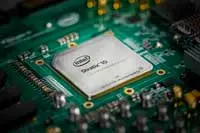 Intel has revealed that it is starting to sample its Stratix 10 FPGA, which uses the company’s 14nm tri-gate (finfet) process.
“Stratix 10 combines the benefits of Intel’s 14nm tri-gate process technology with a revolutionary new architecture called HyperFlex, meeting the performance demands of high-end compute and data-intensive applications ranging from data centres, network infrastructure, cloud computing, and radar and imaging systems,” said Dan McNamara, vp and general manager of the Programmable Solutions Group at Intel.
According to McNamara benefits over the last generation of Stratix include: 2x core performance; 5x the density; up to 70% lower power than Stratix V (equivalent performance); up to 10 TFlops single-precision floating point DSP; up to 1 Tbit/s memory bandwidth with integrated HBM2 (high-bandwidth memory) in-package and Quad-core 64bit ARM Cortex-A53.
McNamara said that Intel sees Stratix 10 as accelerator hardware for data centres and networking.
“As a user’s system demands or hardware requirements change, the FPGA can be reconfigured to accelerate individual tasks, which translates into significant improvements in system-level performance and power efficiency," he explained.
According to McNamara the growing number of bandwidth-intensive applications is creating a massive increase in customer demand and is putting increased pressure on network infrastructures.
"Cisco forecasts that by 2020, nearly a million minutes of video content will cross the network each second, and that by 2020, the number of devices connected to IP networks will be three times the global population.
“Stratix 10 FPGAs will enable network innovations across the access, transmission and networking equipment arenas to aggregate, transport and deliver the triple-play traffic over converged multiservice networks,” McNamara said.
Author
Neil Tyler
Source: www.newelectronics.co.uk
 According to Rice University scientists, two-dimensional materials like graphene may be too flat and hard to stretch to serve in flexible, wearable devices. ‘Wavy’ borophene, an atom-thick layer of boron, might be better, they claim.
The Rice group built computer simulations to analyse the properties of materials which showed that hexagonal vacancies in borophene help soften the material to facilitate its corrugated form.
"Borophene is metallic in its typical state, with strong electron-phonon coupling to support possible superconductivity, and a rich band structure that contains Dirac cones, as in graphene," said theoretical physicist Boris Yakobson.
The team discovered that borophene needs the underlying structure to make it wavy. When grown on a featureless surface, its natural form resembles graphene. According to Yakobson, borophene prefers to be flat because that's where its energy is lowest. But surprisingly, when grown on silver, borophene adopts its accordion-like form while silver reconstructs itself to match. The corrugation can be retained by ‘re-gluing’ boron onto another substrate.
"This wavy conformation so far seems unique due to the exceptional structural flexibility and particular interactions of borophene with silver, and may be initially triggered by a slight compression in the layer when a few too many boron atoms get onto the surface," commented postdoctoral researcher Zhuhua Zhang.
Author
Peggy Lee
Source: www.newelectronics.co.uk
NXP has announced the expansion of its family of automotive motor control MCUs and has introduced a portfolio of hardware, software and integrated motor control solutions designed to speed time to market, simplify system development and shorten design cycles. These additions are said to enable a fully functioning motor system to be up and running in 10 minutes.
“The continued electrification of vehicles is driving growth for electric motors controlling a wide array of automotive systems including fluid pumps, cooling fans, and more,” said Manuel Alves, general manager for NXP’s general purpose and integrated solutions. “MagniV MCUs are engineered to reduce the complexity and time associated with software development, demystifying complex motor control for automotive systems designers across the globe.”
The 17 solutions are single chip, high-voltage MCUs housing the power supply, physical communication layer and application-specific drivers. The solutions also feature advanced development tool enablement technologies such as the Motor Control Development Toolbox, MCAT and FreeMASTER for shorter tuning and debug cycles. New advanced motor control algorithms in the Automotive Math and Motor Control Library support PMSM sensor-less operations in both single and dual-shunt configurations for current sensing.
The S12ZVM MCU family now ranges from 16 to 256kbyte of embedded flash and features new options with onboard physical layer for CAN or High Voltage PWM, while adding more LIN versions for reuse of software and hardware across applications such as pumps and fans.
The S12VR MCU family, which adds 32-pin versions, targets anti-pinch window lift and sunroof applications.
Author
Peggy Lee
Source: www.newelectronics.co.uk
A Dartmouth project called ‘DarkLight’ is said to have demonstrated for the first time how visible light can be used to transmit data even when the light appears dark or off. DarkLight is claimed to provide a new communication primitive similar to infrared communication but it exploits the LED lights already installed rather than needing additional infrared emitters.
"With DarkLight, we can potentially enable light sensing so that it is always on, regardless of the light's illumination status," explained Xia Zhou, assistant professor and co-director of the Dartmouth Networking and Ubiquitous Systems Lab. "DarkLight shows new possibilities on what visible light can do. We believe there are a lot more interesting applications yet to come."
Wireless data is typically beamed through Wi-Fi or Bluetooth, yet the ‘visible light communication’ technology has emerged as a new option. There are limitations, however, due to it being easily blocked or not being able to sustain transmission when light is off.
With DarkLight, light-based communication is sustained even when LEDs emit low luminance, by encoding data into short, imperceptible light pulses, at which point the photodiodes and semiconductor devices convert the light into a current. The DarkLight prototype supports 1.6Kbit/s data rate at 1.8m distance.
According to the researchers, DarkLight could serve as a special mode that ceiling LED lights would switch to so that the light bulbs could still beam data to smart devices in the environment, or alternatively, data could be transmitted from one phone to another, by using the flashlight but without shining a light beam. The technology could potentially offer an alternative for secure communication, since visible light is directional and degrades fast over distance.
Author
Peggy Lee
Source: www.newelectronics.co.uk
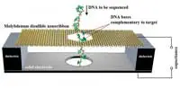 Researchers from the National Institute of Standards and Technology (NIST) have proposed a design for the first DNA sequencer based on an electronic nanosensor that can detect motions as small as a single atom.
The proposed device – a capacitor which stores electric charge – is a ribbon of molybdenum disulfide suspended over a metal electrode and immersed in water. Single-stranded DNA, containing a chain of bases, is threaded through a hole 2.5nm wide in the ribbon. The ribbon flexes only when a DNA base pairs up with and then separates from a complementary base affixed to the hole. The membrane motion is detected as an electrical signal. The DNA sequence is determined by measuring how and when electrical blips vary over time. To detect all four bases, four nanoribbons, each with a different base attached to the pore, could be stacked vertically to create an integrated DNA sensor.
Among other advantages, this material does not stick to DNA, which can be a problem with graphene. The NIST team suggests the method might even work without a nanopore, by passing DNA across the edge of the membrane.
"This approach solves the issue with DNA sticking to graphene if inserted improperly, because this approach does not use graphene," NIST theorist, Alex Smolyanitsky, said. "Another major difference is that instead of relying on the properties of graphene or any particular material used, we read motions electrically by forming a capacitor. This makes any electrically conductive membrane suitable for the application."
According to the team, it made numerical simulations and theoretical estimates to show the membrane would be 79 to 86% accurate in identifying DNA bases in a single measurement at speeds of up to about 70million bases/s.
Author
Peggy Lee
Source: www.newelectronics.co.uk
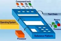 The Towards Ubiquitous Low-power Image Processing Platforms (TULIPP) project has been announced and will receive nearly €4million in funding from Horizon 2020. The initiative will target the development of high performance, energy efficient embedded systems for the growing range of image processing applications.
“Image processing applications stretch across an increasingly broad range of industrial domains and are reaching a higher level of complexity than ever before,” said Philippe Millet of Thales and TULIPP’s project co-ordinator. “The TULIPP reference platform will give rise to advances in system integration, processing innovation and idle power management to cope with the challenges of increasingly complex vision-based systems.”
The TULIPP consortium members include Thales (France) as the project lead and co-ordinator, with Efficient Innovation SAS (France), Fraunhofer IOSB and Ruhr-Universität Bochum (Germany), Hipperos (Belgium), Norges Teknisk-Naturvitenskapelige Universitet (Norway), Sundance Multiprocessor Technology (UK), and Synective Labs (Sweden).
TULIPP will focus on developing a reference platform for vision-based system designers that defines a set of guidelines for the selection of relevant combinations of computing and communication resources while minimising energy consumption and reducing development costs and time-to-market.
In addition, TULIPP will develop three use case demonstrators as proof-of-concept and validation of the reference platform. These use cases will include: a medical imaging surgical X-ray system designed to reduce radiation doses by 75%; a smart automotive embedded vision system for ADAS which, in addition to low-level image processing, interprets what is on the images to deliver safer driving experiences; and an embedded image processing system to create smart drones and unmanned aerial vehicles for the search and rescue of survivors at disaster incidents.
By the end of the project in 2018, TULIPP expects its work to extend by four times the peak performance per Watt of image processing applications and by 10 times the average performance per Watt.
Author
Peggy Lee
Source: www.newelectronics.co.uk