Electronics News
Archive : 13 August 2017 год
 A method to tune the colour of the light emitted by an LED by altering the size of its semiconductor crystals has been discovered researchers from Ludwig-Maximilians-Universitaet (LMU) in Munich and the Johannes Kepler University (JKU) in Austria.
Light-emitting diodes (LEDs) produce light of a defined colour within the spectral range from the infrared to the ultraviolet. The exact wavelength of the emission is determined by the chemical composition of the semiconductor employed.
In the case of some semiconducting materials, the colour can also be tuned by appropriately modifying the size of the crystals of which the light-emitting layer is composed.
The researchers have developed a method for the production of semiconducting nanocrystals of a defined size based on the cheap mineral oxide known as perovskite. These crystals are said to be extremely stable – which ensures that the LEDs exhibit high colour fidelity – and the resulting semiconductors can be printed on surfaces.
Using a scalable and economical electrochemical process, a thin wafer was patterned like a waffle. The depressions served as tiny reaction vessels, whose shape and volume ultimately determined the size of the nanocrystals.
“Our nanostructure oxide layers also prevent contact between the semiconductor crystals and deleterious environmental factors such as free oxygen and water, which limit the working lifetime of the LEDs,” explains JKU Dr Martin Kaltenbrunner.
Author
Peggy Lee
Source: www.newelectronics.co.uk
 A novel design that boosts the power output of chip-mounted terahertz lasers by 80% has been unveiled by researchers at MIT and the University of Toronto.
Applications – including medical and industrial imaging, and chemical detection – depend on small, power-efficient sources of terahertz rays, and the standard method for producing them is said to involve a bulky, power-hungry, tabletop device.
The researchers' design is a new variation on a device called a quantum cascade laser with distributed feedback. Until now, however, the device emitted radiation in two opposed directions. Since most applications of terahertz radiation require directed light, that means that the device squandered half of its energy output.
To counter this problem, the team found a way to redirect 80% of the light that usually exits the back of the laser.
"We increased power without designing a new active medium, which is pretty hard,” said graduate student Ali Khalatpour.
In the waveguide, materials are arranged so that the application of an electric field induces an electromagnetic wave along the length of the waveguide.
The group cut regularly spaced slits into the waveguide, which allow terahertz rays to radiate out. The slits are spaced so that the crests of the waves coincide only along the axis of the waveguide. At more oblique angles from the waveguide, they cancel each other out.
The researchers then simply put reflectors behind each of the holes in the waveguide, a step that they claim can be seamlessly incorporated into the manufacturing process of the waveguide.
The reflectors are wider than the waveguide, and they're spaced so that the radiation they reflect will reinforce the terahertz wave in one direction but cancel it out in the other.
The device has been selected by NASA to provide terahertz emission for its Galactic/Extragalactic ULDB Spectroscopic Terahertz Observatory mission to conduct spectroscopic measurements of oxygen concentrations.
Author
Peggy Lee
Source: www.newelectronics.co.uk
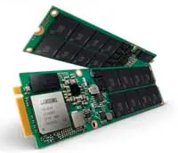 New Vertical NAND (V-NAND) memory solutions and technology have been announced by Samsung which it claims will address the requirements of next generation data processing and storage systems.
According to the company, these solutions will be at the forefront of enabling today’s most data-intensive tasks such as high-performance computing, machine learning, real-time analytics and parallel computing.
“Our highly advanced V-NAND technologies will offer smarter solutions for greater value by providing high data processing speeds, increased system scalability and ultra-low latency for today’s most demanding cloud-based applications,” said Gyoyoung Jin, executive vice president of memory business at Samsung Electronics.
Samsung is sampling the first 16Tbyte next generation small form factor (NGSFF) SSD, which could improve the memory storage capacity and input/output operations per second of today’s 1U rack servers.
Measuring 30.5 x 110 x 4.38mm, the NGSFF SSD is said to increase the storage capacity of a 1U server system by four times compared to using M.2 drives.
The company has also unveiled its first Z-SSD product: the SZ985. The SZ985 is said to require only 15µs of read latency time which the company claims is a seventh of the read latency of an NVMe SSD, as well as reduce system response time by up to 12 times compared to using NVMe SSDs.
Samsung has further introduced a Key Value technology which allows SSDs to process data without converting it into blocks. Instead, Key Value assigns a ‘key’ or specific location to each 'value' or piece of object data – regardless of its size. The key enables direct addressing of a data location, which in turn enables the storage to be scaled-up and scaled-out in performance and capacity. This is said to lead to faster data inputs and outputs and to extend the life of the SSD.
The arrival of a 1Tbit V-NAND chip due next year will enable 2Tbyte of memory in a single V-NAND package by stacking 16 1Tbit dies.
Author
Peggy Lee
Source: www.newelectronics.co.uk
 National Instruments (NI) has unveiled the PXIe-8301 remote control module, the industry’s first solution for laptop control of PXI systems using Thunderbolt 3.
The PXIe-8301 offers PCI Express Gen 3 connectivity through two Thunderbolt 3 ports to maximise performance and can deliver up to 2.3 GB/s of sustained data throughput. Engineers can use the second port to daisy chain additional Thunderbolt 3 or USB-C devices.
According to NI the device’s connectivity and low price point mean that the PXIe-8301 now makes high-performance control of PXI systems more accessible and affordable for engineers performing benchtop characterization and validation or developing portable automated test systems.
“The PXI platform has seen strong adoption with vendors and customers over the past 20 years in a broad set of applications,” said Mark Wetzel, distinguished engineer at NI and technical chair of PXI Systems Alliance. “The introduction of a remote control module using Thunderbolt 3 demonstrates the continued ability of the PXI platform to incorporate the latest commercial technologies and further its reach into high-performance, low-cost and ultraportable applications.”
The PXIe-8301 will help to extend NI’s portfolio for low-cost PXI control, which also includes the recently released embedded PXI Controller, the PXIe-8821. The PXIe-8821 is optimised for test and measurement applications, featuring a 2.6 GHz Intel Core i3-4110E dual-core processor and providing up to 2 GB/s system bandwidth.
Remote control modules and embedded controllers are seen as an important part of the NI platform and ecosystem that engineers can use to build smarter test systems, and which now comprises of over 600 PXI products ranging from DC to mmWave and feature high-throughput data movement using PCI Express bus interfaces and sub-nanosecond synchronization with integrated timing and triggering.
Author
Neil Tyler
Source: www.newelectronics.co.uk
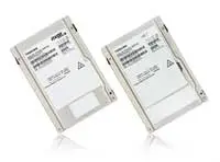 Toshiba Electronics Europe has announced the development of two new flagship enterprise solid state drive (SSD) solutions, the TMC PM5 12Gbit/s SAS series and the CM5 NVM Express (NVMe) series.
Both product lines are built with TMC’s latest 64 layer, 3-bit-per-cell enterprise-class TLC (triple-level cell) BiCS FLASH, making it possible for storage environments to now expand the use of flash with cost-optimised 3D flash memory. Development is expected to be completed in the fourth quarter.
Offering up to 30.72TB, in a 2.5-inch form factor, the TMC PM5 series introduces a full range of endurance and capacity SAS SSDs that will enable data centers to address big data demands while being able to streamline storage deployments. Providing the industry’s first MultiLink SAS architecture, the PM5 series can deliver, according to Toshiba, the fastest performance seen to date from a SAS-based SSD with up to 3,350 MB/s of sequential read and 2,720 MB/s of sequential write in MultiLink mode and up to 400,000 random read IOPS in narrow or MultiLink mode.
The PM5 series’ 4-port MultiLink design is an additional technology to achieve high performance, close to PCI EXPRESS (PCIe ) SSDs, enabling legacy infrastructures to increase productivity without having to be re-architected from the ground up. In addition, PM5 SSDs are able to support multi-stream write technology, a feature that intelligently manages and groups data types to minimise write amplification and minimise garbage collection, which means reduced latency, improved endurance, increased performance and Quality of Service (QoS).
As TMC’s next generation NVMe SSD, the dual-port PCIe Gen3 x4 CM5 is a full-featured enterprise SSD. Like the PM5, it also supports multi-stream write technology. It is NVMe over Fabric-ready with scatter-gather list (SGL) and controller memory buffer (CMB) features. The CMB feature uses a part of DRAM on the SSD as host-system memory, reducing DRAM used load of host-side and it enables high speed as a system.
Using TMC’s BiCS FLASH 64-layer technology, the CM5 series can offer up to 800,000 random read and 240,000 random write IOPS for the 5 DWPD (drive writes per day) model and up to 220,000 random write IOPS for the 3 DWPD model, both with a maximum power draw of 18W.
In addition, the CM5 is being used as a platform to demonstrate and to enable the ecosystem around the Persistent Memory Region (PMR) capability. PMR enables customers to augment system memory with DRAM on the SSD without the use of expensive non-volatile DIMMs (NV-DIMMs). This makes it possible for a single SSD solution to provide both high performance storage and persistent memory to meet system performance requirements, while significantly reducing costs by moving metadata operations, such as logging, journaling and application staging to the SSD.
PM5 12Gbit/s SAS SSDs will be available in capacities ranging from 400GB to 30.72TB with sanitise instant erase (SIE) and Trusted Computing Group (TCG). CM5 NVMe SSDs will offer capacities ranging from 800GB to 15.36TB with SIE and TCG. Both TLC-based product lines offer industry standard endurance ratings with 1, 3 and 5 DWPD options, and the PM5 has a 10 DWPD option available.
Author
Neil Tyler
Source: www.newelectronics.co.uk