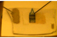
 A bright-light emitting device that is millimetres wide and fully transparent when turned off has been built by a team of engineers at the University of California (UC), Berkeley. The light emitting material is a monolayer semiconductor, which is just three atoms thick.
According to the team, this discovery could pave the way in creating invisible displays – that would be bright when on, but see-through when off – on walls and windows or in applications such as light-emitting tattoos.
"The materials are so thin and flexible that the device can be made transparent and can conform to curved surfaces," said Der-Hsien Lien of UC Berkeley.
The device was developed in the laboratory of professor Ali Javey of UC Berkeley, whose work previously demonstrated that monolayer semiconductors are capable of emitting bright light, but stopped short of building a light-emitting device.
This new work is said to overcome the fundamental barriers in utilising LED technology on monolayer semiconductors, allowing for such devices to be scaled from sizes smaller than the width of a human hair, up to several millimetres. The researchers explained that this means the thickness can be kept small, while the lateral dimensions can be made large to offer higher light intensity.
Commercial LEDs consist of a semiconductor material that is electrically injected with positive and negative charges, which produce light when they meet. Typically, two contact points are used in a semiconductor-based light emitting device; one for injecting negatively charged particles and one injecting positively charged particles. Making contacts that can efficiently inject these charges is a challenge for LEDs, and it is particularly challenging for monolayer semiconductors since there is so little material to work with.
UC Berkeley claimed to have engineered a way to circumvent this challenge by designing device that only requires one contact on the semiconductor.
By laying the semiconductor monolayer on an insulator and placing electrodes on the monolayer and underneath the insulator, the researchers said they could apply an AC signal across the insulator. During the moment when the AC signal switches its polarity from positive to negative (and vice versa), the team explained, both positive and negative charges are present at the same time in the semiconductor, creating light.
The team claimed that this mechanism works in four different monolayer materials, all of which emit different colors of light.
This device is a proof-of-concept, and much research still remains – primarily to improve efficiency, according to the researchers.
Measuring this device's efficiency, however, is not straightforward, but the researchers think it's about 1% efficient. Commercial LEDs have efficiencies of around 25 to 30%.
"A lot of work remains to be done and a number of challenges need to be overcome to further advance the technology for practical applications," Javey said. "However, this is one step forward by presenting a device architecture for easy injection of both charges into monolayer semiconductors."
Author
Bethan Grylls
Source: www.newelectronics.co.uk