At the International Solid-State Circuits Conference 2026 (ISSCC 2026), held February 15–19 in San Francisco, Renesas Electronics presented a series of major advances targeting the software-defined vehicle (SDV) era. The announcements centered on three new SoC technologies for automotive multi-domain electronic control units (ECUs) and a configurable ternary content-addressable memory (TCAM) architecture built on a 3-nm FinFET process.
Chiplet Architecture With ASIL D Safety Across Dies
One of the central challenges for next-generation automotive SoCs is maintaining functional safety in chiplet configurations, where multiple silicon dies communicate over high-speed interfaces. Renesas addressed this by developing a proprietary architecture that pairs the industry-standard UCIe die-to-die interface with a RegionID-based access control mechanism.
Standard UCIe implementations do not transmit RegionIDs between chiplets. Renesas solved this by mapping RegionIDs into physical address space, encoding them into the UCIe region, and passing them between dies. This approach allows memory management units and real-time cores to enforce safe resource access across chiplets, achieving Freedom from Interference (FFI) as required under ASIL D. Testing confirmed that the UCIe interface reaches transfer speeds of 51.2 GB/s, approaching the practical ceiling for intra-SoC communication.
AI Processing Quality and Zero-Defect Clock Management
As neural processing units (NPUs) take on larger roles in automotive SoCs, their footprint has grown by roughly 1.5x compared to previous generations, introducing new clock distribution challenges. Renesas tackled this by integrating test circuits directly into the hierarchical clock pulse generator (CPG) structure and unifying the signal paths for user and test clocks.
In test mode, upper- and lower-level modular CPGs synchronize to a single clock source, enabling consistent phase adjustment across the entire chip. The result is automotive-grade zero-defect quality even for large-scale 3-nm SoC designs - a critical requirement for SDV deployments where software complexity continues to escalate.
Advanced Power Gating: Over 90 Domains, 13% Lower IR Drop
Power efficiency and safety go hand in hand in high-performance automotive chips. Renesas implemented over 90 independent power domains in the new SoC, enabling fine-grained control ranging from a few milliwatts up to tens of watts depending on the active workload.
Power switches are divided into ring and row structures. During power-up, ring switches suppress inrush current while row switches equalize domain impedance. Together, these techniques reduce IR drop by approximately 13% compared to conventional designs. For functional safety, the dual-core lockstep (DCLS) configuration assigns independent power switches and controllers to master and checker cores, so a failure on either side is immediately detected through lockstep operation.
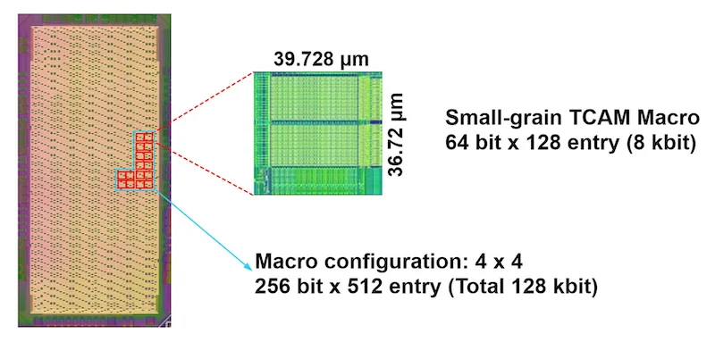
3-nm TCAM: High Density, Low Power, Functional Safety
Alongside the ECU-focused SoC work, Renesas announced a configurable TCAM built on a 3-nm FinFET process. TCAM enables parallel search operations essential for routing, filtering, and real-time decision-making - capabilities that grow more important as vehicles process data from dozens of sensors simultaneously.
The architecture supports flexible key widths and entry depths, allowing it to be tuned for specific automotive use cases. On the safety front, Renesas addressed a historical limitation of SECDED ECC in TCAM: because bitcells at the same address are physically adjacent, double-bit soft errors were traditionally uncorrectable. Renesas mitigated this by splitting odd and even data buses to increase physical separation between user data and parity bits, converting potential double-bit errors into correctable single-bit events. A dedicated SRAM for ECC parity with an independent address decoder further improves detection of incorrect-address writes.
R-Car X5H: Bringing It All Together
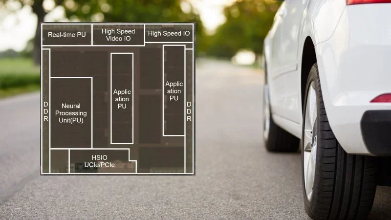
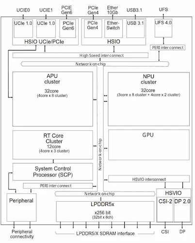
These technologies are being incorporated into the R-Car X5H, Renesas's flagship fifth-generation automotive SoC and the industry's first multi-domain automotive chip manufactured on a 3-nm process. The device is capable of simultaneously handling advanced driver assistance systems (ADAS), in-vehicle infotainment (IVI), and gateway functions within a single chip. Renesas has already begun shipping silicon samples and evaluation boards alongside the R-Car Open Access (RoX) Whitebox SDK to select customers and partners, including Bosch and ZF.
With both the SoC technologies and the 3-nm TCAM now entering productization, Renesas is laying the architectural groundwork for centralized compute, heterogeneous chiplet integration, and memory systems optimized for performance and ISO 26262 compliance in the vehicles of the next decade.