 Researchers from MIT have reported the first chip-fabrication technique that they claim could enable significantly different materials to be deposited in the same layer. They also report that, using the technique, they have built chips with working versions of all the circuit components necessary to produce a general-purpose computer.
The layers of material in the researchers’ experimental chip measure between one and three atoms thick. This work could aid efforts to manufacture thin, flexible, transparent computing devices, which could be laminated onto other materials. “The methodology is universal for many kinds of structures,” said Xi Ling, form the MIT’s Research Laboratory of Electronics. “This offers us tremendous potential with numerous candidate materials for ultrathin circuit design.”
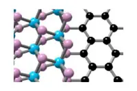
Previously, only materials with closely matched lattices have been deposited laterally in the same layer of a chip. The researchers’ experimental chip however, uses molybdenum disulphide and graphene, two materials with different lattice sizes.
To assemble their laterally integrated circuits, the researchers first deposit a layer of graphene on a silicon substrate. Then they etch it away in the regions where they wish to deposit the molybdenum disulfide. Next, at one end of the substrate, they place a solid bar of a material known as PTAS.
They heat the PTAS and flow a gas across it and across the substrate. The gas carries PTAS molecules with it that stick to the exposed silicon but not to the graphene. Wherever the PTAS molecules stick, they catalyse a reaction with another gas that causes a layer of molybdenum disulfide to form.
The technique also has implications for the development of the ultralow-power, high-speed computing devices known as tunnelling transistors and, potentially, for the integration of optical components into computer chips.
Because electron tunnelling is immune to the thermal phenomena that limit the efficiency of conventional transistors, tunnelling transistors can operate at very low power and could achieve much higher speeds.
Author
Tom Austin-Morgan
Source: www.newelectronics.co.uk