
Electronics News
Archive : 11 December 2014 год
 Two modified Raspberry Pi's will be sent into space with British astronaut Tim Peake next year, as part of a school coding competition organised by UK Space and the European Space Agency.
The Astro Pi Competition invites primary and secondary school children to submit ideas and write code for space experiments that can be done using the two credit card sized computers, with the ultimate aim to encourage interest in coding and spacecraft engineering among the younger generation.
Speaking at the launch event, UK Space Agency CEO David Parker said: "Our project is a part of a much bigger challenge and that is to prepare young people for the challenges of the 21st century.
"Most of the jobs that are foreseen to be created by the UK's booming space industry in the upcoming years won't be about designing and building spacecraft, they will be about using data, about making software to control space missions. The experience with the level of precision and accuracy the children will get when writing code for Raspberry Pi is exactly what one needs for success of any space mission."
In the primary school age category, teams will be asked to devise and describe an original idea for an experiment or application which can be conducted on the Astro Pi by Peake during his mission. The two best submissions will get the opportunity to work with the Astro Pi team to interpret their ideas and the team at the Raspberry Pi Foundation will then code them ready for flight.
In the secondary school age group, the competition will be run across three age categories, one for each of Key Stages 3, 4 and 5 . In the first phase, competitors can submit their ideas for experiments and applications. The best 50 submissions in each age category will win a Raspberry Pi computer and an Astro Pi board on which to code their idea.
In phase two, all teams will develop code based on their original concept and two winning teams will be selected in each age category. The winning teams' code will be readied for flight by the Raspberry Pi Foundation and CGI.
The Astro Pi competition will be officially launched in January, with the first teams selected in April 2015 ahead of Tim Peake's November launch.
Author
Laura Hopperton
Source: www.newelectronics.co.uk
 Looking to address a verification challenge that is compared to navigating through London's traffic on a bad day, Cadence Design Systems has launched the Perspec System Verifier platform
The platform brings together an intuitive graphical specification of system level verification scenarios and a definition of the SoC topology and actions. It is said by the company to automate system level coverage driven test development using constraint solving technology. An increase in productivity of up to ten times is claimed over manual test development. The increase in productivity is said to help designers to reproduce, find and fix complex bugs to improve overall SoC quality.
Frank Schirrmeister, pictured, director of product management and marketing in the Cadence System and Verification Group, said: "We are seeing shifts in verification approaches from 'brute force' to hardware verification logic to metric driven. This new platform adds scenario and software driven verification.
"Verification is like navigating through London's traffic," he noted. "You need to know which streets are one way, what difference the time of day makes and so on. It's the same in the chip world."
Perspec requires users to create abstract description in C to test various scenarios. "The output," said Schirrmeister, "is a set of tests which can run on a range of platforms, including FPGA based verification. It enhances top down testing."
Amongst Perspec's features are:
* A UML based view of system level actions and resources that creates a view of complex and hard to test interactions
* Solver technology to automate the generation of portable tests, and
* Tests that run on all pre silicon verification platforms.
Concluding, Schirrmeister said: "Perspec allows you to take two use cases, assess them and generate tests to make sure that, for example, cache coherency works during the power up and power down cycles."
Author
Graham Pitcher
Source: www.newelectronics.co.uk
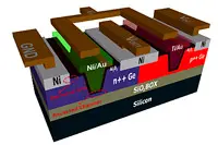 Researchers at Purdue University in the US have created what they believe is the first modern germanium circuit. The CMOS device is unusual in that it uses Ge as the semiconductor, instead of silicon.
Germanium was originally the semiconductor of choice in the early days of the transistor – and Purdue was instrumental in its creation in 1947 by providing purified germanium. However, Ge was superseded by silicon. Now, with silicon transistors reaching a scaling limit, Ge is being considered as a replacement for silicon.
Previously, germanium has been limited to p-type devices. However, in recent work, Purdue researchers have shown that Ge can be used to create n-type transistors and hence CMOS electronic devices. The team will present its findings at the forthcoming International Electron Devices Meeting in San Francisco.
By doping germanium and then etching away the top layer, recessed channels are created which serve as gates, allowing the transistors to switch on and off.
According to the team, the fundamental part of the device – the inverter – is the best performing non silicon inverter demonstrated so far, with a gain of 36V/V.
Germanium based devices have been fabricated with channel lengths as small as 20nm and the research has also addressed NAND and NOR logic gates.
Author
Graham Pitcher
Source: www.newelectronics.co.uk
 The IEEE International Electron Devices Meeting (IEDM) – the leading forum for the presentation of advances in microelectronic, nanoelectronic and bioelectronic devices – will celebrate its 60th anniversary when it gets underway next week in San Francisco.
"The IEDM conference has long been the place where the world's experts have presented breakthroughs in transistors, memory devices and related semiconductor technologies," said Suman Datta, IEDM 2014 publicity chair and Professor of Electrical Engineering at Penn State University. "The tradition of attracting the best speakers and a large, diverse audience from around the world continues as we mark the conference's 60th anniversary, with an added focus on emerging areas of importance where semiconductor technology is expected to play an expanding and enabling role."
More than 200 papers will be presented, including two particularly interesting pieces of research by IBM and the Japanese LEAP project.
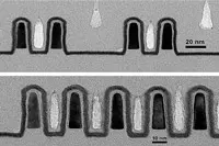
The IBM paper addresses the challenge of creating FinFETs on advanced processes. According to the research team, high density fin formation is one of the most critical processes in the FinFET device fabrication flow. Because each fin in the device must be nearly identical, any new process must be able to form fins with a high degree of structural precision.
IBM's researchers are looking at directed self assembly using block copolymers (BCP) and 193nm immersion lithography to make FinFETs for beyond the 10nm node. The team has created a topographic template pattern in which the BCP is confined between the sidewalls of the template, driving the pattern into registry with the surface topography. Fins created at a pitch of 29nm are said to show good uniformity, with no signs of gross variation in critical dimensions.
The image shows, at the top, groups of two fins formed by the process, while, at the bottom, is a cross section of a larger group of fins.
Meanwhile, work continues to develop memory technologies which will support advanced manufacturing processes. There has been much research into phase change memory, in which a chalcogenide is shifted between its crystalline and amorphous states to represent a 0 or a 1. However, a team from LEAP – the Low Power Electronics Association and Project – believes it has created a superior approach, which it calls topological switching RAM, or TRAM
In this approach, data is stored according to the movement of Ge atoms in a GeTe/Sb2Te3 crystal superlattice. TRAM is said to require up to 20 times less programming energy than a chalcogenide based approach.
Author
Graham Pitcher
Source: www.newelectronics.co.uk