
Electronics News
Archive : 17 February 2015 год
 New materials that could yield higher computational speeds and lower power consumption are being researched by a team from the University of Michigan and Western Michigan University.
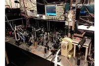
Because most modern circuits rely on controlling electronic charge, which can be disrupted, spintronics, may offer a more robust alternative. However, making a radiation resistant spintronic device requires a material that can maintain its spin-dependence after it has been irradiated. The Michigan research team believes bulk silicon doped n-GaAs could be the answer.
Studying spintronic materials required the research team to combine two well established fields: spin dynamics; and radiation damage. Both tool sets are robust, but combining the two required sifting through the wealth of radiation damage research.
Technically, the Michigan team has measured the spin properties of n-GaAs as a function of radiation fluence using time resolved Kerr rotation and photoluminescence spectroscopy. Results show the spin lifetime and g-factor of bulk n-GaAs is largely unaffected by proton irradiation, making it a candidate for further study for radiation resistant spintronic devices. The team will also study other spintronic materials and prototype devices after irradiation, since it believes there are plenty of questions to tackle.
Author
Graham Pitcher
Source: www.newelectronics.co.uk
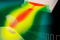 A solid state technology platform developed by scientists in Italy and France is said to open the door to the use of THz photonics in a range of applications.
While there has been much research into THz technology, the team says one missing piece has been a complementary detection technology. To solve this problem, the researchers used an approach that exploits the excitation of plasma waves in the channel of field effect transistors (FET). Alongside creating the first FET detectors based on semiconductor nanowires, the team also developed the first THz detectors made of mono- or bilayer graphene.
"Our work shows that nanowire FET technology is versatile enough to enable 'design' via lithography of the detector's parameters and its main functionalities," said Miriam Serena Vitiello, leader of the Terahertz Photonics Group in the Nanoscience Institute at CNR and Scuola Normale Superiore.
According to the team, the nanowire detector operates at room temperature and can detect frequencies in excess of 3THz, with maximum modulation speed in the MHz range.
The team now plans to 'push the device's performance in the ultrafast detection realm', as well as integrating nanowire detectors with THz quantum cascade microlasers. Vitiello noted: "This will allow us to take THz photonics to a whole new level of 'compactness' and versatility, where it can finally begin to address many 'killer' applications."
Author
Graham Pitcher
Source: www.newelectronics.co.uk
 Globalfoundries has announced a partnership with imec under which they will jointly research future radio architectures and designs for highly integrated mobile devices and IoT applications.
"This collaboration expands our relationship with imec and we're eager to leverage its R&D expertise in RF technology to accelerate time-to-volume of designs and deliver leading edge RF technology to our customers," said Peter Rabbeni, director of RF segment marketing at Globalfoundries.
According to the companies, a key challenge for next generation mobile devices is controlling the cost and footprint of the radio and antenna interface circuitry. A typical mobile device must support up to 28 bands today, with more complex carrier aggregation schemes and additional frequency bands are expected for future generations. These challenges, they continue, are driving the need for an agile radio that integrates many of the separate components into one piece of silicon, including power amplifiers, antenna switches and tuners. The partners are also looking for a flexible, low cost solution.
Author
Graham Pitcher
Source: www.newelectronics.co.uk
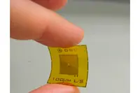 GE Global Research has made what it says is a significant technological achievement in the development of a sensor capable of detecting 'chemicals of interest' at low concentrations.
Working with the Technical Support Working Group, Quantum Magnetics and KemSENSE, the company has used its RFID technology to develop battery free RFID tags coated with a sensing material that responds to explosives and oxidisers. The tag, which can be deployed on a variety of surfaces, will change its electronic properties in the presence of such chemicals and send an alert to a reader.
Sensors which can detect ultra-trace levels of chemicals could also have application in industries beyond security. According to GE, they could be used to detect gas leaks degradation of electrical isolation and bacterial growth in buildings. In healthcare, the sensors could be used to ensure that surfaces have been cleaned properly.
Radislav Potyrailo, a principal scientist at GE Global Research, said: "In airports today, bulky, stationary desktop systems typically screen for explosives. Suspicious surfaces are swabbed and analysed, consuming substantial time, space and power. Compared to a conventional desktop detector, our system is 300 times smaller and reduces weight and power use 100 fold. It simplifies detection by using an individual sensor, rather than relying on arrays of multiple sensors."
Author
Graham Pitcher
Source: www.newelectronics.co.uk
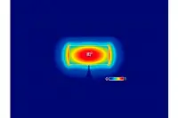 Scientists from Ghent University and imec have seen a peculiar interaction between light and sound in a nanoscale area. The work is said to hold the prospect on enhanced signal processing being integrated on mass producible silicon photonic chips.
Silicon photonics builds on structures called silicon photonic wires, which carry optical signals from one point to another at the speed of light, with the light trapped inside the wire by total internal reflection. Confining light is one thing, says the team, but manipulating it is another.
Reporting in Nature Photonics, the team says it managed not only to confine light, but also sound in silicon nanowires, with the sound oscillating at 10GHz. According to the team, it realised the sound could not be trapped in the wire by total internal reflection, so the scientists sculpted the environment of the core to make sure any vibrational wave trying to escape it would actually bounce back. Doing so, they confined both light and sound to the same nanoscale waveguide core.
Because they are trapped in a small area, the light and vibrations strongly influence each other: light generates sound and sound shifts the colour of light – a process known as stimulated Brillouin scattering.
This interaction was exploited to amplify specific colours of light and the researchers anticipate this demonstration could open new ways to manipulate optical information; for instance, light could be converted into sonic pulses and back into light – thereby implementing delay lines.
Author
Graham Pitcher
Source: www.newelectronics.co.uk