
Electronics News
Archive : 20 February 2015 год
 With demand for cellular data continuing to rise and outdoor small cells seen as an essential element in the long-term delivery of high-capacity urban networks, TTP has developed a small cell designed specifically for deployment on lamp posts. The eNodeB is said to fit a lamp post's standard photocell socket, providing speedy installation without any modification to the lighting column or its power supply.
"There has been a lot of focus on the unit cost of small cells, but less attention has been paid to total cost of deployment," said TTP's Steve Baker. "The costs of site acquisition, planning consents and installation become significant factors when tens or even hundreds of thousands of small cells are considered. The TTP outdoor lamp post cell addresses these challenges head-on."
TTP's prototype eNodeB – based on Freescale's BSC9131 QorIQ Qonverge processor – will be shown at Mobile World Congress next month. It incorporates 4G/LTE Access Point software from ip.access and has been demonstrated with the Quortus EPX Core evolved packet core. The device, which is targeted at 50m cells, is designed to support up to 32 active users and to provide downlink rates of up to 100Mbit/s.
Author
Graham Pitcher
Source: www.newelectronics.co.uk
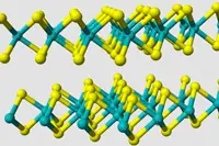 The interest in two dimensional materials continues to grow as researchers look to explore potential replacements for silicon in electronic devices.
In the latest development, researchers at the University of Pennsylvania have have found a new way to make molybdenum disulphide (MoS2). The attraction of MoS2 over graphene is that it has a band gap and can emit light. According to the team, growing flakes of the material around 'seeds' of molybdenum oxide makes it easier to control the size, thickness and location of the material.
"Everything we do with regular electronics, we'd like to be able to do with two dimensional materials," said Professor Charlie Johnson. "Graphene has one set of properties that make it very attractive for electronics, but it lacks this critical property, being able to turn on and off. Molybdenum disulphide gives you that."
The team's advance is in developing a way that allows MoS2 flakes to be made using chemical vapour deposition, but also by 'seeding' the substrate with a precursor.
"We start by placing a small amount of molybdenum oxide in the locations we want," said researcher Carl Naylor, "then we flow in sulphur gas. Under the right conditions, those seeds react with sulphur and flakes of molybdenum disulphide being to grow."
Prof Johnson added: "Because we grow it where we want it, we can make devices more easily. We have all of the other parts of the transistors in a separate layer that we snap down on top of the flakes, making dozens and potentially even hundreds, of devices at once. Then we were able to observe that we made transistors that turned on and off like they were supposed to and devices that emit light like they are supposed to."
The research is also said to represent the first steps in creating a new family of 2D materials. "We can replace molybdenum with tungsten and sulphur with selenium," Naylor said, "and just go down the periodic table from there. We can imagine growing all of these different materials in the places we choose and taking advantages of all of their different properties."
Author
Graham Pitcher
Source: www.newelectronics.co.uk