
Electronics News
Archive : 26 February 2015 год
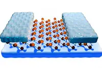 A European research project says it has made an important step towards the further miniaturisation of nanoelectronics using silicene, a semiconducting material which combines the properties of silicon and graphene.
"Electronics are currently embedded in many layers of silicon atoms," explained Dr Athanasios Dimoulas, coordinator of the EU's 2D-NANOLATTICES project. "If they can be manufactured in a single layer, they can be shrunk down to much smaller sizes and we can cut down on power leakage, at the same time making devices more powerful and energy efficient."
The project's breakthrough has been to make a Field Effect Transistor (FET) from silicene that can operate at room temperature. However, there are issues with the material as its properties are modified when it comes into contact with other substances. In its work, the project grew silicene on a silver substrate, then transferred it to silicon dioxide. "Tests showed that performance of silicene is very, very good on the non-metal substrate," Dr Dimoulas added.
"The fact that we have this one transistor made of just one single layer of material like silicon has not been done before and this is really something that can be described as a breakthrough. On the basis of this achievement, it could be possible to make transistors up to 100 times smaller in the vertical direction," he continued. He also believes lateral dimensions can be reduced, with the overall prospects of a unit area accommodating up to 25times more electronics than is currently possible.
Author
Graham Pitcher
Source: www.newelectronics.co.uk
 According to newly launched company Semitrex, it typically takes more than 14 different parts to make a power supply. It believes this 'pieces and parts' approach – where numerous semiconductor parts are embedded on several circuit boards – has yielded only marginal increases in energy efficiency to date.
In a move which it says disrupts the existing dynamic, Semitrex has incorporated almost every part necessary to make a power supply for circuits or chargers into one module.
"Everyone is looking for better energy efficiency," noted Michael Freeman, Semitrex' CEO and CTO. "Our muxcapacitor cascading technology uses capacitive, rather than inductive, conversions for the primary voltage reduction. This permits us to create the first comprehensive power conversion breakthrough the industry has seen in decades, which produces the highest energy efficiencies and the lowest standby power draws.
"Our TRONIUM power supply system on a chip requires less than 1mW of standby power to stay ready to respond to the next current demand."
Designed around an ASIC, TRONIUM is a multichip module whose output can be set between 1.8V and 48V. According to Semitrex, it uses an approach called Capacitive Voltage Reduction to produce efficiencies of more than 90% at all loads.
Author
Graham Pitcher
Source: www.newelectronics.co.uk
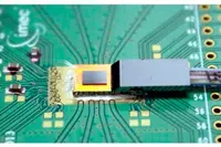 In a joint presentation at the International Solid State Circuits Conference (ISSCC), imec, Tyndall National Institute, University of Leuven and Ghent University described a 4 x 20Gbit/s wavelength division multiplexing hybrid CMOS silicon photonics transceiver. The development, say the partners, paves the way to cost effective, high density single mode optical fibre links.
The device comprises a silicon photonics chip, flip chip integrated with a low power 40nm CMOS chip. The photonics chip, fabricated on imec's 25Gbit/s Silicon Photonics Platform, has an array of four 25Gbit/s ring modulators, coupled to a common bus waveguide to allow WDM transmission. On the receive side, a ring based demultiplexing filter with a channel spacing of 300GHz is connected to an array of four 25Gbit/s Ge waveguide photodetectors.
The CMOS chip includes four differential 20Gbit/s ring modulator drivers and four 20Gbit/s transimpedance amplifiers. A 12 channel single mode fibre array is packaged onto the chip's grating coupler array, using a planar approach developed at Tyndall National Institute.
According to the partners, error free operation was demonstrated in a 20Gbit/s loop-back experiment for all four WDM channels, as well as with two channels running together. Dynamic power consumption was found to be less than 2pJ/bit. The partners claim the transceiver can be further scaled to higher bandwidth capacity by adopting more advanced CMOS technology and by adding more WDM channels.
Author
Graham Pitcher
Source: www.newelectronics.co.uk