
Electronics News
Archive : 27 May 2015 год
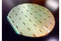
 In an effort said to be aimed at alleviating the environmental burden posed by electronic devices, a team of researchers from the University of Wisconsin-Madison has worked with the US Department of Agriculture's Forest Products Laboratory (FPL) to develop a semiconductor chip made almost entirely of wood.
The research team, led by UW-Madison Professor Zhenqiang Ma, has explored the feasibility of replacing the chip's substrate with cellulose nanofibril (CNF), a flexible, biodegradable material made from wood.
"The majority of material in a chip is support," said Prof Ma. "We only use less than a couple of microns for everything else. The chips are so safe you can put them in the forest and fungus will degrade them; they become as safe as fertilizer."
FPL project leader Zhiyong Cai noted: "If you take a big tree and cut it down to the individual fibre, the most common product is paper. The dimension of the fibre is in the micron stage. But what if we could break it down further to the nano scale? At that scale, you can make very strong and transparent CNF paper."
Cai's group addressed two key barriers to using wood derived materials in electronics – surface smoothness and thermal expansion. "You don't want it to expand or shrink too much. Wood is a natural hydroscopic material and could attract moisture from the air and expand," Cai says. "With an epoxy coating on the surface of the CNF, we solved both the surface smoothness and the moisture barrier."
The group's work also demonstrates a more environmentally friendly process that showed performance similar to existing chips. Most of today's wireless devices use gallium arsenide based chips, but gallium arsenide can be environmentally toxic, particularly in the massive quantities of discarded electronics.
Yei Hwan Jung, a graduate student in electrical and computer engineering, said the new process can greatly reduce use of the material. "I've made 1500 GaAs transistors in a 5 x 6mm chip. Typically, for a microwave chip that size, there are only eight to 40 transistors – the rest of the area is just wasted.
"We take our design and put it on CNF using a deterministic assembly technique and make a completely functional circuit with performance comparable to that of existing chips."
Prof Ma concluded: "Mass producing chips is so cheap and it may take time for the industry to adapt to our design. But flexible electronics are the future and we think we're going to be well ahead of the curve."
Author
Graham Pitcher
Source: www.newelectronics.co.uk
 Researchers from EPFL's Integrated Systems Laboratory, working together with the organisation's Radio Frequency Integrated Circuit group, have developed a biosensor chip featuring six sensors, a control unit and a radio transmission module.
According to EPFL, the biosensor chip – which would be implanted just beneath the skin – can monitor simultaneously the concentration of a number of molecules, including glucose and cholesterol, and certain drugs.
The device uses an induction coil to draw power from an external battery attached to the skin by a patch. "A simple plaster holds together the battery, the coil and a Bluetooth module used to send the results immediately to a mobile phone," said EPFL's Dr Sandro Carrara.
"This is the world's first chip capable of measuring not just pH and temperature, but also metabolism related molecules like glucose, lactate and cholesterol, as well as drugs," Dr Carrara continued.
However, the development is in its early days and clinical tests may not take place on humans for another three years.
"Knowing the precise and real time effect of drugs on the metabolism is one of the keys to the type of personalised, precision medicine that we are striving for," said Dr Carrara.
Author
Graham Pitcher
Source: www.newelectronics.co.uk
 According to Qualcomm's president Derek Aberle, the company is now looking to grow its presence in the burgeoning Internet of Things (IoT) market significantly.
Speaking at an event held by Qualcomm in San Francisco, Aberle said the industry needed technology leaders with the right scale and resources if the Internet of Everything, as the company refers to the IoT, is to deliver value to individuals, communities and companies.
Qualcomm, long associated with the smartphone market, is looking to firmly establish itself in this growing market and, while the chip maker has been working in the IoT sector for the past few years, Aberle said that it would now be looking to push much harder into the market as it unveiled a number of new products.
"Qualcomm is well-positioned to provide advanced connectivity, computing and interoperability for devices and machines," he said. "Our technologies are already driving this new era of intelligent connectivity and computing and we plan to invest heavily in these emerging segments."
Rivals Samsung, IBM and Intel have all released IoT-enabled chips and Intel revealed that it was investing more than $3billion in building its own IoT business unit.
To emphasise the scope and range of Qualcomm's presence, Aberle used his presentation to describe the companies work in a variety of projects, including smart cities – covering areas such as municipal Wi-Fi, water use, recycling, lighting, transportation, energy and infrastructure – as well as in connected healthcare, where Qualcomm Life, the company's mobile health unit, now has around 500 customers and collaborators.
The company is also heavily involved in developing wearable devices and, according to Aberle, 'more than 20million connected vehicles are currently deployed globally with Qualcomm Snapdragon LTE and 3G modems'.
Last year, the company generated more than $1billion from supplying the IoT market, said Aberle.
Aberle also talked about the company's 'vision' for the IoT.
"We want to make devices so smart that they do not have to be connected to the Internet to be controlled by individuals; instead, the device should learn and adapt to scenarios. If the devices are smarter, much more of the computing can be done at the device, instead of up in the cloud."
The size of the IoT market is open to debate and, depending on the definition of the market, estimates of its worth range from $1bn to almost $20bn this year.
Aberle said that, whatever the figure, the opportunities for companies like Qualcomm were enormous and the importance of first mover advantage would be significant. "We're determined that Qualcomm will take a big slice of the pie for itself," he suggested.
Qualcomm used the event to launch two new chips. It is hoping the QCA401x and QCA4531 will spur development of IoT products.
The QCA401x is Qualcomm's flagship IoT chip and is intended to be used to power devices such light bulbs, smart TVs, cameras and other gadgets. The QCA4531, which is a Linux based Wi-Fi device, will act as a hub between larger devices like media servers and appliances.
"Across the board, our technologies are supporting the Internet of Everything, whether through more intelligent connectivity or computing. To ensure success we need to not only provide a range of solutions to what is a very diverse market but better understand how connectivity will drive a much deeper market engagement," Aberle concluded.
Author
Tom Austin-Morgan
Source: www.newelectronics.co.uk
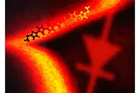 Researchers at Columbia University in New York say they have developed a technique that allows the creation of a single molecule diode. The team adds that its molecular diodes perform 50 times better than all prior designs.
Researchers at Columbia University in New York say they have developed a technique that allows the creation of a single molecule diode. The team adds that its molecular diodes perform 50 times better than all prior designs.
Latha Venkataraman, associate professor of applied physics, who directed the work, said: "Our approach created a single molecule diode that has high rectification (more than 250) and an 'on' current of about 0.1µA. Constructing a device where the active elements are only a single molecule has long been a tantalising dream in nanoscience."
Since a diode acts as a valve, its structure needs to be asymmetric so that electricity flowing in one direction experiences a different environment than electricity flowing in the other direction. To achieve this, the team has designed molecules with asymmetric structures.
"While such asymmetric molecules display some diode like properties, they are not effective," explains Brian Capozzi, a PhD student working with Venkataraman. "A well designed diode should only allow current to flow in the 'on' direction and it should allow a lot of current to flow in that direction. Asymmetric molecular designs have typically suffered from very low current flow in both directions and the ratio of current flow in the two has typically been low."
To overcome these issues, Venkataraman's team focused on developing an asymmetry around the molecular junction by surrounding the active molecule with an ionic solution. They also used gold metal electrodes of different sizes to contact the molecule.
"It's amazing to design a molecular circuit, using concepts from chemistry and physics, and have it do something functional," Venkataraman said. "The length scale is so small that quantum mechanical effects are absolutely a crucial aspect of the device. So it is a triumph to be able to create something that you will never be able to physically see and that behaves as intended."
Venkataraman and her team are now working to understand the fundamental physics behind their discovery and to increase the rectification ratios using new molecular systems.
Author
Graham Pitcher
Source: www.newelectronics.co.uk
 IDT and EPC have announced that they are collaborating to develop technology based on gallium nitride (GaN). Under the agreement, the partners will explore how EPC's eGaN technology can be integrated with IDT's products.
"GaN offers exciting opportunities to develop higher performance, differentiated products for our customers," said Sailesh Chittipeddi, IDT's chief technology officer. "I look forward to exploring how GaN-based products, with all their inherent benefits, may be brought to market in the not-so-distant future."
The two companies are looking to address three market sectors. In communications and computing applications, GaN's low capacitance and zero QRR, coupled with the low inductance of a chip scale package, is said to result in high efficiency at high frequency and IDT plans to use this increase in efficiency to improve power density. Meanwhile, the partners are looking to GaN to improve the adoption of wireless power, as well as to create a portfolio of RF products for the communications infrastructure market.
"A growing number of companies, such as IDT, are integrating GaN technology into their solutions as a way to move beyond the limitations of silicon," said Alex Lidow, ceo of EPC. "Our team looks forward to working alongside IDT engineers to bring the speed and efficiency of EPC's GaN technology to IDT customers."
Author
Tom Austin-Morgan
Source: www.newelectronics.co.uk
 The Carrefour hypermarket in Lille, France has replaced its fluorescent lighting with 2.5km of LED lighting from Philips that can also transmit location signals to a shopper's smartphone, triggering an app to provide location based services.
The system in operation at the hypermarket comprises 800 linear LED fixtures that use Visible Light Communication technology to transmit a unique code that can be detected by a smartphone's camera. The Philips system enables Carrefour to help shoppers to navigate their way around the 7800m² store and to find promotions. The positioning technology is said to be accurate to within 1m, while the LED lighting will reduce the total lighting-based electricity consumption of the hypermarket by 50%.
"We are always on the lookout for innovations to facilitate customers' navigation in our stores and meet consumers' expectations," Céline Martin, director of Commercial Models and Innovation for Carrefour hypermarkets, said: "Thanks to this application, we are now able to provide our customers with a new service, enabling them to quickly search and locate their preferred promotions or detect all the promotions around them when in-store."
* For more on VLC, see http://www.newelectronics.co.uk/electronics-technology/can-leds-help-to-solve-the-looming-spectrum-congestion-problem/59424/
Author
Tom Austin-Morgan
Source: www.newelectronics.co.uk
 Risk is the biggest issue facing semiconductor manufacturers, according to Professor Asen Asenov, the Glasgow University academic who is also chief executive of Gold Standard Simulations (GSS), which specialises in predictive simulation of nano CMOS devices.
Risk is the biggest issue facing semiconductor manufacturers, according to Professor Asen Asenov, the Glasgow University academic who is also chief executive of Gold Standard Simulations (GSS), which specialises in predictive simulation of nano CMOS devices.
"We are trying to help the industry to narrow their technology options," he said. "Simulation helps them to reduce their exposure to risk – and there are big risks in choosing technology. It's a good time for an agile company like GSS."
GSS's focus is beyond the 10nm node, where Prof Asenov believes the best candidate is nanowire transistors – also known as gate all round transistors – which are likely to scale to the 5nm node. "But 5nm is likely to be the end of scaling," he said. "Beyond that, it's likely to be physically impossible."
Prof Asenov sees nanowire transistors as 'better designed FinFETs'. "FinFETs cover three of the four sides of the channel, so are better than MOSFETs. Nanowire transistors cover all four sides of the channel, which means less leakage and more drive current. And they may not be so difficult to make."
But at these dimensions, quantum effects come into play. "Quantum mechanics play a big role, so our software includes features that allow users to simulate very accurately the performance of these transistors," said Prof Asenov.
GSS' GARAND simulator is being offered as a way for manufacturers to explore the way forward. "Each variant will take money to develop, so companies look to use simulation as much as possible to reduce their exposure to risk. If you try to experiment, it's very expensive and takes a long time. Bad decisions can take you in the wrong direction."
However, working at the 5nm node will not be for the faint hearted. "Few big companies will remain," Prof Asenov believes. "Those that do will get all the business; it will be much like Boeing and Airbus." However, he doesn't see one foundry dominating. "That company would be too powerful; there will be two or three."
Author
Graham Pitcher
Source: www.newelectronics.co.uk