
Electronics News
Archive : 23 June 2015 год
 While FinFET based chips have finally begun to enter the market, the technology may be too rich for many companies' tastes as the cost-per-function decreases promised by Moore's Law bottom out.
Speaking at a panel during the Design Automation Conference, Scott McCormack, Freescale's director of SoC design, said the team approached its first finFET project 'with an abundance of caution because of the cost [of design]'.
"I don't think it was such a game-changer, but we found a lot more attention to detail was needed, compared to 28nm. We saw a lot of demand on compute resources."
Pressure on server time came from the need to run many more simulations towards the end of the project to check the circuitry would meet timing under different variations of voltage, temperature and process. The use of double patterning to define the routing between transistors – and the effects of random nanometre-scale offsets between masks in a pair – also increased the number of simulated 'corners'. Some companies reported running more than 100 'corners' on their FinFET designs, while those working on older processes, such as 40nm, used fewer than 10.
"We haven't gone through the exercise of reducing the number of corners," McCormack continued. "As the process matures, we can start to move down that path."
Afshin Montaz, senior engineering manager of Broadcom's mixed signal design group, said: "16nm is not for every product or application; the cost per transistor has gone up compared to 28nm, so you may not win on cost. The main advantage of 16nm is speed, which may make sense, or if you want to reduce power drastically."
McCormack agreed: "You don't go into 16nm FinFET to save money: we wanted to differentiate on power. But the cost is a whole new game."
The power advantage of FinFET largely lies in its greatly improved static dissipation. Jayonta Lahiri, vp of engineering in ARM's physical design group, said: "Leakage is much more under control: you really have on/off states again."
Benjamin Mbouombouo, design lead and power solutions architect at Avago, said leakage is 10% of what it was on 28nm. Improved drive currents, compared to the older planar transistor, made it possible to use narrower devices to support high clock speeds, but higher gate capacitance – caused by coupling between the many fins and their surroundings – increases switching power dissipation.
Despite the apparent cost concerns, TSMC technology manager Willy Chen said more companies are signing up for FinFET designs. "We are expecting 50 product tapeouts by the end of this year."
Take one chip and and wait for results
The realisation that silicon dissolves slowly in water could lead to a new class of medical sensor, Professor John Rogers claimed in a keynote at this year's DAC.
Prof Rogers' team has combined silicon with magnesium oxides and silk to build water soluble sensors. One such device, that measures pressure and temperature for monitoring brain injuries, has started testing in rats. Although the team has not yet been able to build wireless transmitters into the devices, molybdenum wires lead from the cranium to an external transmitter.
"The platform is absorbable on the timescale of a week," Prof Rogers said. If successful, the biodegradable sensors will make it possible to avoid the need to perform a second surgery after treatment for brain injuries.
Author
Chris Edwards
Source: www.newelectronics.co.uk
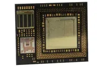 Freescale says it has introduced the smallest single chip module (SCM) for IoT applications, integrating components which would otherwise have been housed on a 6in board in a package measuring 17 X 14 X 1.7mm.
Called the i.MX 6Dual SCM, the device is enabled for DDR memory and integrates an i.MX 6Dual applications processor, power management integrated circuit, flash memory, embedded software/firmware and system level security technology.
"Early stage companies entering the IoT and portable markets often work with limited resources and must create novel, compelling products in highly constrained form factors," said Nancy Fares, Freescale's vp of system solutions. "For these and other businesses targeting highly competitive and fast-growing markets, Freescale's SCM product line represents a major breakthrough that addresses a host of hardware and software design challenges, allowing them to begin development immediately and focus their efforts on designing highly differentiated applications and products."
SCM products will be delivered as a fully tested and software enabled platform for consumer and industrial applications, supporting Linux and Android.
Initial availability of the i.MX 6Dual SCM is planned for August 2015, with further products planned for release over the next two years.
Author
Graham Pitcher
Source: www.newelectronics.co.uk
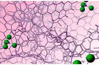 Researchers from the University of Cambridge, together with French collaborators based in Toulouse, have developed a method that allows the inside of supercapacitors to be viewed at the atomic level. The team says this approach could be used in order to optimise and improve the devices.
By using a combination of nuclear magnetic resonance (NMR) spectroscopy and scales sensitive enough to detect changes in mass of a 1µg, the researchers could visualise how ions move around in a supercapacitor. They found that, while charging, different processes are at work in the two identical pieces of carbon 'sponge' which function as the electrodes.
Dr John Griffin, a postdoctoral researcher in the Department of Chemistry, said: "[Supercapacitors are] much better at absorbing charge than batteries, but since they have much lower density, they hold far less of that charge. Being able to see what's going on inside these devices will help us to control their properties, which could help to make them smaller and cheaper, and that might make them a high power alternative to batteries."
When a supercapacitor is being charged, ions 'stick' to the surface' when being discharged, they 'hop' off the surface and move back into the electrolyte.
"To increase the area for ions to stick to, we fill the carbon electrode with tiny holes, like a carbon sponge," said Dr Griffin. "But it's hard to know what the ions are doing inside those holes."
In their study, the researchers used NMR to look inside functioning supercapacitors to see how they charge and store energy and an electrochemical quartz crystal microbalance to measure changes in mass.
From the two sets of information, the researchers built a precise picture of what happens inside a supercapacitor while it charges.
"In a battery, the two electrodes are different materials, so different processes are at work," said Dr Griffin. "In a supercapacitor, the two electrodes are made of the same porous carbon sponge, so you'd think the same process would take place at both – but it turns out the charge storage process is more complicated than we previously thought."
The experiments showed the two electrodes behave differently: in the negative electrode, positive ions are attracted to the surface as the supercapacitor charges. But in the positive electrode, an ion 'exchange' happens, as negative ions are attracted to the surface, while at the same time, positive ions are repelled.
The team will now try to understand why different ions behave differently on charging and attempt to design systems with higher performance.
Author
Graham Pitcher
Source: www.newelectronics.co.uk