
Electronics News
Archive : 7 July 2015 год
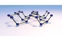 Research conducted by McGill University and Université de Montréal is said to provide further evidence that black phosphorus could be a strong candidate for use in chips of the future.
The researchers have found that when electrons move in a phosphorus transistor, they do so only in two dimensions. "Transistors work more efficiently when they are thin, with electrons moving in only two dimensions," says Thomas Szkopek, an associate professor in McGill's Department of Electrical and Computer Engineering.
When separated into single atomic layers, black phosphorus is known as phosphorene. Unlike graphene, black phosphorus can be readily switched on and off.
"To lower the operating voltage of transistors, and thereby reduce the heat they generate, we have to get closer and closer to designing the transistor at the atomic level," Szkopek says. "The toolbox of the future for transistor designers will require a variety of atomic layered materials – an ideal semiconductor, an ideal metal and an ideal dielectric. All three components must be optimised for a well designed transistor and black phosphorus fills the semiconducting material role."
In order to determine how electrons move in a phosphorus transistor, the researchers observed them under the influence of a magnetic field in experiments performed at the US National High Magnetic Field Laboratory. "What's surprising in these results is that the electrons are able to be pulled into a sheet of charge which is two dimensional, even though they occupy a volume that is several atomic layers in thickness," Szkopek says. That is said to be significant because it could potentially facilitate manufacturing the material – though Szkopek notes that 'no one knows how to manufacture this material on a large scale'.
"There is a great emerging interest around the world in black phosphorus," Szkopek says. "We are still a long way from seeing atomic layer transistors in a commercial product, but we have now moved one step closer."
Author
Graham Pitcher
Source: www.newelectronics.co.uk
 RN Electronics has become one of the first Test Houses in the UK to be UKAS accredited to EN55032 (CISPR32), the new standard for electronics described as Multimedia Equipment (MME). EMC (electromagnetic) testing is already taking place on a range of professional audio equipments to the new standard.
"We have a number of clients in the Professional Audio and IT equipment sectors. This new standard will make their life much easier when it comes to testing" said Roger Ray, technical director of RN Electronics.
MME are electronic products that incorporate a range of functions that include those in Audio equipment, Video equipment, Information Technology Equipment (ITE), and Broadcast receiving equipment. MME also covers entertainment lighting control equipment as well as combinations of all these equipment types.
EN55032 has been developed to address the fact that modern day ITE equipment now integrates many different functions and capabilities; these were previously assessed by different standards. Before, a PC with built in TV receiver, CD player and camera had to have each of these elements tested separately, the EN55032 standard now covers all those types of equipment.
Pic: Testing at RN Electronics to EN55032 of a Studer Vista X Broadcast Audio Console.
Author
Tom Austin-Morgan
Source: www.newelectronics.co.uk
 Scientists at the University of Warwick have developed the 'Q-Eye', a sensor that is said to be much faster than competing technologies used to detect and identify hidden objects. The invention senses radiation across the terahertz band of the electromagnetic spectrum, just between the infrared and microwave bands.
Professors in Warwick's Nano-Silicon Group, Physics Department, Evan Parker and Terry Whall, led the team which developed the device. Prof Parker commented, "We were very surprised when our first very crude prototype showed such impressive speed and detection performance and our initial calculations indicated world-beating detector capability."
The Q-Eye features a thin film of aluminium deposited on top of a silicon layer placed under strain, used to create an electronic cooling (e-cooling) process. The electrons in the silicon layer are so isolated from the silicon lattice they become highly sensitive to incoming radiation. This e-cooling process is the secret to Q-Eye sensor's performance, enabling fast imaging and material identification.
The device could prove useful in discovering concealed goods in the retail industry or for non-destructive monitoring, for example quality control in drugs or food. Other applications include astronomical and climate science observations, detecting weapons in airport security and medical diagnosis.
Professors Parker and Whall are currently working on a demonstrator of the device, having been awarded a £100,000 Smart award from Innovate UK. The work is moving out of academic research into the commercial world, offering opportunities for partnership and investment.
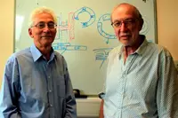
Pic: Prof Terry Whall and Prof Evan Parker, creators of the Q-Eye
Author
Tom Austin-Morgan
Source: www.newelectronics.co.uk
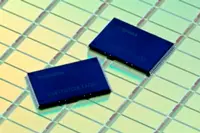 Toshiba has announced a method of embedding flash memory based on 65nm logic process that uses less power than current mainstream technology, and a single-poly non-volatile memory (NVM) process based on 130nm logic and analogue power. Applying the optimal process to various applications will allow Toshiba to expand its product line-up in such areas as microcontrollers, wireless communication ICs, motor controller drivers and power supply ICs.
There is demand in the IoT market for low power consumption in areas including wearable and healthcare-related equipment. Toshiba has adopted Silicon Storage Technology's third-generation SuperFlash cell, in combination with its own 65nm logic process technology. Microcontrollers for consumer and industrial applications that apply the process are said to consume 60% less power than that of current mainstream technology.
Following the first series of microcontrollers, Toshiba plans to release sample Bluetooth Low Energy products, as well as apply the 65nm process to its wireless communication IC product family that can optimise use of low power consumption characteristics, including contactless cards.
As well as developing products for IoT, the company also aims to lower power consumption for entire systems, targeting 50µA/MHz operation. In applications where significant cost reductions are a concern, Toshiba claims it has developed an NVM embedded process that adopts Yield Microelectronics Corporation's single-poly multi-time programmable cells on Toshiba's 130nm logic process technology. This is said to improve performance while limiting increased steps in mask pattern lithography to three or fewer.
Author
Tom Austin-Morgan
Source: www.newelectronics.co.uk
 Researchers at MIT and the University of British Columbia claim to have found a promising new approach to delivering the short, but intense, bursts of power needed by wearable electronic devices. The trick, they say, is to use yarns made from niobium nanowires 140nm in diameter as the electrodes in tiny supercapacitors – pairs of nanowires with an insulator between them.
"Imagine you've got some kind of wearable health monitoring system," says Professor Ian Hunter from MIT, "and it needs to broadcast data, for example using Wi-Fi, over a long distance." At the moment, the coin sized batteries used in many small electronic devices have very limited ability to deliver a lot of power at once, which is what such data transmissions need.
"Long distance Wi-Fi requires a fair amount of power," says Prof Hunter, "but it may not be needed for very long. We know it's a problem experienced by a number of companies in the health monitoring or exercise monitoring space. So an alternative is to go to a combination of a battery and a capacitor." A battery caters for long term, low power functions, while the capacitor provides short bursts of high power. Such a combination should be able to either increase the range of the device or reduce its size.
Ideally, Prof Hunter says, it is desirable to have high volumetric power density and high volumetric energy density. "Nobody's figured out how to do that," he says. However, he adds that, with the new approach: "We have fairly high volumetric power density, medium energy density and low cost."
Niobium is abundant and widely used, so the team believes the whole system should be inexpensive and easy to produce. Other groups have made similar supercapacitors using carbon nanotubes or other materials, but the MIT team believes niobium yarns are not only stronger, but also 100 times more conductive, allowing niobium based supercapacitors to store up to five times as much power in a given volume as carbon nanotube versions.
Although the material has been only been produced in the lab, the team is now working on how to design a practical, easily manufactured version.
Author
Graham Pitcher
Source: www.newelectronics.co.uk
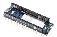 The Arduino Yun WiFi microcontroller board has been redesigned in a more compact housing so that it can be used with a breadboard. This is said to make prototyping easier.
Called the Yun Mini – and available from RS Components – the board has approximate PCB dimensions of 70 x 23mm, less than half the area required by the Arduino Yun PCB. This makes it suitable for use in small spaces, including home automation projects.
The Yun Mini features an ATmega32u4 microcontroller and the Qualcomm Atheros AR9331 SoC, which includes a MIPS 24K CPU running at up to 400MHz. A bridge library enables communication between the two processors, providing Arduino programs running on the ATmega with the ability to run shell scripts, communicate with network interfaces and receive information from the AR9331 processor.
With IEEE802.11b/g/n Wi-Fi running at up to 150Mbit/s, there are 20 digital I/O, seven of which can be used as PWM outputs and 12 as analogue inputs. Other specifications include a 16MHz crystal oscillator, a micro-USB connector, an ICSP header, two reset buttons and one user button.
Author
Graham Pitcher
Source: www.newelectronics.co.uk
 The AMALTHEA4public project is attempting to develop more powerful computers and complex software for autonomous vehicles to help them become more intelligent. The project, headed up by Bosch, comprises a team of 21 international technology specialists looking to develop embedded systems with central processing units that work in parallel.
Today, new vehicles are said to contain around 70 embedded systems which monitor and regulate certain driving functions. The trend towards automated driving means that individual computers have to run more software and the overall system is becoming more complex.
The programs that industry is currently using to develop embedded systems are not designed to incorporate parallel computing with multi- and many-core (over eight cores) processors. To make optimum use of the new hardware, developers will have to divide the software up and assign it to the various cores.
The AMALTHEA4public project team is establishing a methodology for this and setting up a comprehensive software platform. With the help of this open source tool platform, it is claimed engineers will be able to develop multi- and many-core systems for their applications.
The platform is based on Eclipse, another open-source development environment, and is available free of charge to anyone who wishes to use it. The consortium will set up an Eclipse project and community that will support the developers and keep them in touch with each other even after the project has finished. This should make the outcome of AMALTHEA4public available to a wider circle and establish it as the standard for developing embedded multi- and many-core systems.
Author
Tom Austin-Morgan
Source: www.newelectronics.co.uk
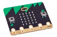 The BBC has officially launched micro:bit, a codeable computer that will be distributed free of charge in October to every child in year 7 or the equivalent across the UK.
The device, part of the BBC's Make It Digital initiative, is intended to build on the heritage of the BBC Micro by inspiring young people to get creative and to develop a new generation of 'inventors and pioneers'.
Tony Hall, director general of the BBC sais: "Channelling the spirit of the Micro for the digital age, the BBC micro:bit will inspire a new generation in a defining moment for digital creativity here in the UK. All you need is your curiosity, creativity and imagination – we'll provide the tools. This has the power to be transformative for the UK. The BBC is one of the few organisations in the world that could convene something on this scale, with such an unprecedented partnership at its core."
First conceived by BBC Learning in 2012, micro:bit is the result of a collaboration between 29 partners, including ARM, element14, Freescale, Nordic Semiconductor and Samsung. Measuring 4 x 5cm, the device will be available in a range of colours. It connects to other devices, sensors, kits and objects and is said to be a companion to Arduino, Galileo, Kano, littleBits and Raspberry Pi.
Key features of micro:bit are said to include: 25 red LEDs; two programmable buttons; an accelerometer; a compass; Bluetooth Smart connectivity; and five I/O rings.
Each element of the micro:bit is said to be programmable and support will be available later in the summer via a dedicated website (microbit.co.uk).
Author
Graham Pitcher
Source: www.newelectronics.co.uk
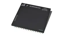 Freescale has licensed Rochester Electronics to provide a continuing manufacturing solution for its MC68040 32bit microprocessor product family. The agreement between Freescale and Rochester provides customers of the legacy MPUs with access to a secure and reliable source of parts for continued product supply after Freescale announced the discontinuation of the devices.
In addition to the 68040 family, Rochester legacy support includes 68020, 68030, 68060 and the 68882 floating point coprocessor. Freescale will also be supporting Rochester on the supply of the MC68360 QUICC communications processor.
Chris Gerrish, president of Rochester Electronics said: "The MC680x0 family of products has been and will continue to be critical to many systems. Rochester's capability to continue production will save customers immeasurable redesign costs, time and effort."
First released in 1990, the MC680x0 family was used in Apple Macintosh, Amiga and Alpha Microsystems computers. They are said to have been widely used in sectors including military, aerospace, transportation, medical, industrial and communications, all of which are characterised by long installed product lifetimes and the need for extended availability of component parts. Rigorous qualification and standards approval processes can make redesign of systems in these areas either difficult or prohibitively expensive.
Author
Tom Austin-Morgan
Source: www.newelectronics.co.uk
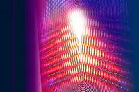 Harvard researchers have created surface plasmon wakes on a metallic surface and claim they can be controlled and steered. The team believes their work could lead to new types of plasmonic couplers, as well as lenses that could create two dimensional holograms or focus light at the nanoscale.
"The ability to control light is a powerful one," said Professor Federico Capasso, from Harvard's School of Engineering and Applied Science. "Our understanding of optics on the macroscale has led to holograms, Google Glass and LEDs, just to name a few technologies. Nano-optics is a major part of the future of nanotechnology and this research furthers our ability to control and harness the power of light on the nanoscale."
Surface plasmons are confined to the surface of a metal. In order to create wakes through them, Prof Capasso's team designed a faster than light running wave of charge along a one dimensional metamaterial.
The metamaterial – a nanostructure of rotated slits etched into a gold film – changes the phase of the surface plasmons generated at each slit relative to each other, increasing the velocity of the running wave. The nanostructure also acts like a boat's rudder, allowing the wakes to be steered by controlling the speed of the running wave.
The team discovered that the angle of incidence of the light shining onto the metamaterial provides an additional measure of control and, by using polarised light, the direction of the wake can be reversed.
Pic: Daniel Wintz, Patrice Genevet, and Antonio Ambrosio
Author
Graham Pitcher
Source: www.newelectronics.co.uk