
Electronics News
Archive : 14 July 2015 год
![]() A team of physicists from Germany, the US and Japan says it has used a scanning tunnelling microscope (STM) to create a transistor consisting of one molecule and a small number of atoms. The team says the device's action is 'markedly different' from that which might be expected and claims this could be important for future such devices.
A team of physicists from Germany, the US and Japan says it has used a scanning tunnelling microscope (STM) to create a transistor consisting of one molecule and a small number of atoms. The team says the device's action is 'markedly different' from that which might be expected and claims this could be important for future such devices.
The team used a STM to create a transistor consisting of a single organic molecule and positively charged metal atoms, all positioned on the surface of an indium arsenide crystal. Kiyoshi Kanisawa, a physicist at NTT-BRL, used the growth technique of molecular beam epitaxy to prepare this surface.
Subsequently, the researchers assembled electrical gates from the metal ions, then placed the molecule at various desired positions close to the gates. Stefan Fölsch, a physicist at the Paul-Drude-Institut für Festkörperelektronik (PDI), who led the team, said: "The molecule is only weakly bound to the InAs template. So, when we bring the STM tip very close to the molecule and apply a bias voltage, single electrons can tunnel between template and tip. In our case, the charged atoms nearby provide the electrostatic gate potential that regulates the electron flow and the charge state of the molecule."
According to the team, the 'perfection and reproducibility' offered by these STM generated transistors will enable the exploration of elementary processes involving current flow through single molecules at a fundamental level. The researchers believe that understanding and controlling these processes – and the new kinds of behaviour to which they can lead – will be important for integrating molecule-based devices with existing semiconductor technologies.
Alongside PDI, the team included the Freie Universität Berlin, NTT Basic Research Laboratories and the US Naval Research Laboratory.
Pic: STM image of a phthalocyanine molecule inside 12 indium atoms on an InAs surface. PDI
Author
Graham Pitcher
Source: www.newelectronics.co.uk
 As part of the Government's Summer Budget, the Chancellor, George Osborne, confirmed funding for six new multidisciplinary research centres, worth a total of £45million, which will drive forward the UK's Digital Economy research, knowledge and skills.
The £23m investment will come via The Engineering and Physical Sciences Research Council and will support the centres over the next five years. The centres will be hosted by the Universities of York, Bath, and Nottingham, Swansea University, UCL and Newcastle University.
"This latest investment demonstrates our commitment to maximising the digital revolution for the UK," Universities and Science Minister Jo Johnson said. "These Centres will lead the way in developing innovative digital products which enhance our daily lives - from personalised digital health services to the use of interactive media in education."
The centres will focus on a wide variety of areas and potential applications, such as improving motion capture technology, refining the ethical use of personal data, designing technology for interactive media, health, social care and cybersecurity and to help rebalance the national economy.
They will build on the UK's existing academic strengths, grow and develop the pool of interdisciplinary trained researchers and work together to help position the country as a world leader in Digital Economy research.
Pic: Universities and Science Minister Jo Johnson
Author
Tom Austin-Morgan
Source: www.newelectronics.co.uk
 Globalfoundries has unveiled the 22FDX platform, said to deliver FinFET-like performance and energy efficiency at a cost comparable to 28nm planar technologies. It claims the process could provide an optimal solution for IoT, RF connectivity and networking products.
The fully depleted silicon on insulator (FD-SOI) process has an operating voltage of 0.4V, along with 20% smaller die size than a 28nm process. It also requires 10% fewer masks and nearly half as many immersion lithography layers.
"The 22FDX platform enables our customers to deliver differentiated products with the best balance of power, performance and cost," said Sanjay Jha, CEO. "In an industry first, 22FDX provides real-time system software control of transistor characteristics: the system designer can dynamically balance power, performance and leakage. Additionally, for RF and analogue integration, the platform delivers best scaling combined with highest energy efficiency."
Four 'flavours' of 22FDX are being introduced: the ultra low power 22FD-ulp; the ultra high performance 22FD-uhp; the ultra low leakage 22FD-ull; and 22FD-rfa for RF analogue designs.
Jean-Marc Chery, STMicroelectronics' chief operating officer said: "Globalfoundries' FDX platform, using an advanced FD-SOI transistor architecture developed through our long standing research partnership, confirms and strengthens the momentum of this technology by expanding the ecosystem and assuring a source of high-volume supply. FD-SOI is an ideal process technology to meet the always on, low power requirements of IoT and other power sensitive devices worldwide."
Pic: Sanjay Jha, CEO, Globalfoundries
Author
Graham Pitcher
Source: www.newelectronics.co.uk
 As process nodes shrink, the problem of feature variations is increasing. Looking to address the issue, Applied Materials has unveiled the Centris Sym3 etch system. The tool is said to feature an entirely new chamber and to enable what the company calls atomic level precision manufacturing.
Centris Sym3 uses the company's True Symmetry technology, which offers multiple tuning controls that allow processes to be optimised to the atomic level.
One of the key features is the ability to control and remove etch byproducts, which mitigates such problems as line edge roughness, pattern loading and defects.
According to global product manager Amulya Athayde, there are three main challenges: the need for uniformity across the wafer; how to get better dice, with all different features, different pattern densities; and how to deal with variation as designs feature tighter line widths and double patterning.
"In a few years, we'll be down to a couple of atoms variation," he said. "Even now, you can count the atoms. Meanwhile, higher aspect ratios
mean we have to get ions into smaller features and effectively."
The company says it has created features with an aspect ratio of 30:1 on advanced processes. This is achieved by tight control of gas flow, RF plasma and temperature. "The gas has to be distributed evenly and the wafer temperature needs to be uniform," Athayde added. "It'a big challenge getting these factors to work together."
Author
Graham Pitcher
Source: www.newelectronics.co.uk
 Renesas Electronics and Audi have established a strategic relationship which not only addresses the traditional automotive control areas powertrain, chassis, body and safety, but also newer applications, including automated drive, connected car and the electrical vehicle.
Ricky Hudi, head of electric/electronic development at Audi, said: "I'm pleased that we have Renesas as an innovative, quality conscious and reliable partner working with us on our Progressive SemiConductor Program. We will join forces to increase the processing performance, comfort level and intelligence of our cars even further."
Audi's Progressive SemiConductor Program is designed to make the latest semiconductor technologies available in cars more effectively, while increasing reliability. An important part of this is said to involve joint developments with semiconductor companies.
"We are pleased to be able to work on this program as a strategic partner with Audi," said Ryuji Omura, Renesas' executive vice president. "The collaboration with Audi serves as an important opportunity for Renesas to gain deeper understanding of the European automotive marketplace."
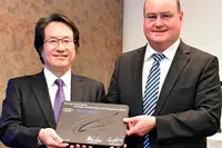
Pic: Left, Ryuji Omura, Renesas, and Ricky Hudi, Audi
Author
Graham Pitcher
Source: www.newelectronics.co.uk
 Plessey Semiconductors has announced that it will be leading a £1.3million government funded project in conjunction with AIXTRON Ltd and Bruker Nano Surfaces Division. Plessey claims this project will accelerate high volume manufacturing of its LEDs created with GaN-on-Silicon technology.
The department for Business, Innovation and Skills launched the Advanced Manufacturing Supply Chain Initiative (AMSCI) to improve the global competitiveness of UK advanced manufacturing and supply chains as well as to encourage major suppliers to locate in the UK. Through the AMSCI funding twenty supply chain projects from across the country will profit from a total of £67m of government investment. There is £109m being invested in the same projects by industry.
"This project supports the work we have ongoing with AIXTRON and Bruker to further increase the yield of our GaN-on-Silicon process," Dr. Keith Strickland, Plessey cto, said. "These improvements are required as part of our move to 200mm silicon substrates.
"A 200mm wafer has almost twice the usable area of our existing 150mm wafers and therefore will almost double the number of LEDs produced for the same relative cost."
Author
Tom Austin-Morgan
Source: www.newelectronics.co.uk