
Electronics News
Archive : 11 August 2015 год
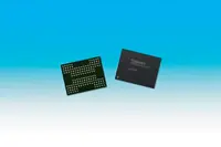 Toshiba has announced the development of a 16-die (max.) stacked NAND flash memory that uses Through Silicon Via (TSV) technology. The prototype will be shown at the Flash Memory Summit 2015, being held in Santa Clara, USA.
Traditional stacked NAND flash memories are connected together with wire bonding in a package, while TSV technology uses the vertical electrodes and vias to pass through the silicon dies for the connection. This enables high-speed data input and output, and reduces power consumption.
According to Toshiba the TSV technology is capable of achieving an I/O data rate of over 1Gbps which is higher than any other NAND flash memories with a low voltage supply: 1.8V to the core circuits and 1.2V to the I/O circuits and approximately a 50% power reduction of write operations, read operations, and I/O data transfers.
This new NAND flash memory provides a solution for low latency, high bandwidth and high IOPS/Watt in flash storage applications, including high-end enterprise SSD.
A part of this applied technology was developed by the New Energy and Industrial Technology Development Organization (NEDO).
Author
Neil Tyler
Source: www.newelectronics.co.uk
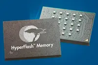 Cypress Semiconductor has expanded its NOR HyperFlash product line with the qualification of a new 256Mb memory capable of delivering up to 333 MBps of read bandwidth. The 3.0V S26KL256S HyperFlash device is the latest addition to the industry’s first flash memory family that supports the high-bandwidth, low-pin-count HyperBus interface.
The device is intended for high-performance applications, such as automotive instrument clusters, industrial automation, communication systems, and medical equipment, which require very high read bandwidth to enable the fastest boot time for instant-on requirements, along with a low-pin-count interface to reduce package size and PCB cost.
Running at frequencies up to 166MHz, HyperFlash products can achieve Double-Data-Rate (DDR) read bandwidths as high as 333 MBps for 1.8V products and 200 MBps for 3.0V products. The device is offered in a 48-mm2 24-ball package and is capable of operating in an extended temperature range of -40ºC to +125ºC.
The HyperFlash memory family offers 3.0V and 1.8V versions and includes three densities: 128Mb, 256Mb and 512Mb and have been designed to provide a seamless migration path from Quad SPI to dual Quad SPI to HyperFlash memory, allowing system applications to be scaled to different levels of flash performance when paired with compatible controllers.
"With the trend toward instant-on systems for automotive, industrial and communication applications, we are seeing more and more interest from chipset manufacturers for the high-bandwidth, low-pin-count HyperBus interface, and increased demand from our customers in these segments for our HyperFlash and HyperRAM memories," said Hiro Ino, Senior Director of the NOR Flash Product Family at Cypress. "Our new 3.0V, 256Mb HyperFlash device is part of our plan to provide a range of voltage and density options to help meet this demand."
Author
Neil Tyler
Source: www.newelectronics.co.uk