
Electronics News
Archive : 30 September 2015 год
 Researchers in the Laboratoire d’analyse et d’architecture des systèmes (LAAS-CNRS) in Toulouse and the INRS in Quebec claim to have developed an electrode material that means electrochemical capacitors produce results similar to batteries, yet retain their particular advantages.
With the development of on-board electronic systems and wireless technologies, the miniaturisation of energy storage devices has become necessary. Micro-batteries are widespread and store a large quantity of energy due to their chemical properties. However, they are affected by temperature variations and suffer from low electric power and limited lifetime. By contrast, micro-supercapacitors have high power and theoretically infinite lifetime, but only store a low amount of energy.
Micro-supercapacitors have been the subject of an increasing amount of research, but no concrete applications have come from it. Their lower energy density has meant that they were not able to power sensors or microelectronic components. The French and Canadian researchers have succeeded in removing this limitation by combining the best of micro-supercapacitors and micro-batteries.
They have developed an electrode material whose energy density is said to exceed all the systems available to date. The electrode is made of an extremely porous gold structure into which ruthenium oxide has been inserted. These expensive materials can be used in this application because the components are in the order of square millimetres.
This electrode was used to make a micro-supercapacitor with energy density 0.5J/cm², which is about 1000 times greater than existing micro-supercapacitors, and very similar to the density characteristics of current Li-ion micro-batteries.
With this energy density, their long lifetime, high power and tolerance to temperature variations, these micro-supercapacitors could finally find used in wearable, intelligent, on-board microsystems.
Author
Tom Austin-Morgan
Source: www.newelectronics.co.uk
 Microsoft has announced the Microsoft Azure Certified for IoT programme, an ecosystem of partners whose offerings have been tested and certified so businesses can take their next IoT project from testing to production more quickly. Current partners include BeagleBone, Freescale Intel Corporation, Raspberry Pi, Resin.io, Seeed Technology, and Texas Instruments.
"We live in a connected world, and the intelligent cloud is powering it all," said Scott Guthrie, executive vice president of Microsoft's Cloud + Enterprise Division. "As data and devices continue to proliferate, there is vast opportunity for businesses to tap into their data to make their applications more intelligent. Through our offerings across applications, data and IoT, and cloud infrastructure, we are enabling companies to innovate more easily and rapidly, using the tools and platforms they know and love."
Microsoft’s Azure IoT Suite is said to integrate with a company's existing processes, devices and systems to build and scale IoT projects using preconfigured solutions.
Barb Edson, general manager, Data Platform and IoT, for Microsoft added: “Microsoft Azure Certified for IoT helps companies to quickly implement the right hardware and software through verified interoperability for these devices.”
To further enable designers to better manage their data Microsoft has also announced the expansion of Azure Data Lake. This includes Azure Data Lake Analytics, Azure Data Lake Store, the U-SQL programming language, and Azure HDInsight. Azure Data Lake is claimed to make big data processing and analytics simpler and more accessible.
Pic: Scott Guthrie, executive vice president of Microsoft's Cloud + Enterprise Division
Author
Tom Austin-Morgan
Source: www.newelectronics.co.uk
 Plessey is to invest £60million to expand its LED manufacturing facility in Plymouth. The expansion will increase production capacity by a factor of 30, triple the workforce and put Plessey in a position to capture what it calls a ‘significant share’ of the growing market for solid state lighting market.
Michael LeGoff, Plessey’s CEO, noted: “We are entering a very exciting period for the company with our new technology and products gaining traction in one of the fastest growing technology markets. The expansion is not only significant for the company, but also for British high tech manufacturing. It aligns well with national strategies, such as the Growth Review, that support manufacturing and make the UK a global leading exporter of high value goods.”
The move, which will see Plessey increase its manufacturing capacity to more than 3billion mm2 of GaN material per year, has been supported by a £30m loan from Deutsche Bank and £6.7m from the Regional Growth Fund. The expansion should be completed by the end of 2017.
According to a report from MarketsandMarkets, demand for solid state lighting is projected to reach $22.2billion by 2020, driven by high brightness LEDs.
Author
Graham Pitcher
Source: www.newelectronics.co.uk
 STMicroelectronics has licensed ARM’s 32bit ARMv8-R processor technology and will deploy it in 32bit MCUs targeting real time safety related smart driving applications, as well as in industrial applications.
According to the company, the first implementations of the ARMv8-R processor will be in multicore devices for powertrain, safety and gateway applications.
“As a lead partner of ARM’s automotive optimised microcontroller technology, ST is continuing to pave the way to delivering products that enable every facet of smart driving,” said Marco Monti, general manager of ST’s automotive product group. “ST will continue to support and develop its successful current 32bit MCU platform, while beginning the transition to the ARM architecture.”
Automotive MCUs employing the ARMv8-R architecture are expected to deliver best in class real time performance and functional safety features, combined with innovations for sensing, computation and actuation. The architecture offers virtualisation and separation to improve software reliability, reduce development costs and enable consolidation of multiple applications onto one smart processing platform.
James McNiven, general manager of ARM’s CPU group, said: “ST has extensive automotive experience and deep customer relationships. Its transition to the ARMv8-R architecture will be a significant boost in ensuring it is well positioned for continuing success in this highly competitive market.”
Author
Graham Pitcher
Source: www.newelectronics.co.uk
 The full service foundry division of ams has added the H35 process to its platform. The 0.35µm high voltage CMOS process is said to offer voltage scalable transistors, allowing area and performance improvements.
The transistors are optimised for drain-source voltage levels ranging from 20V to 100V, with significantly lower on-resistance. According to ams, an optimised 30V NMOS transistor in power management applications can replace a fixed 50V transistor, with an area saving of about 50%. Meanwhile, a 60V optimised NMOS device requires 22% less area than a standard 120V NMOS transistor. By using less area, foundry customers can benefit from more dice per wafer, ams points out.
Area optimised devices are suited to a range of applications, including MEMS drivers, motor drivers, switches and power management ICs.
“Being among first foundries worldwide offering true voltage scalable devices, proves ams’ expertise in developing speciality high voltage CMOS processes and in providing excellent manufacturing services,” said Markus Wuchse, general manager of ams’ full service foundry division. “Our hitkit, the ams benchmark Process Design Kit, as well as our high voltage process expertise, enable our partners to optimise their HV integrated circuits towards area and on-resistance, which immediately results in more dice per wafer.”
The H35 process expands the company’s ‘More Than Silicon’ portfolio, which provides a package of technology modules, IP, cell libraries, engineering consultancy and services to help customers develop advanced analogue and mixed signal circuits.
Author
Graham Pitcher
Source: www.newelectronics.co.uk
 The IQS series of coherent optical receivers, from Teledyne LeCroy, is said to feature the industry’s highest bandwidth. The company says that, when combined with its LabMaster 10Zi-A oscilloscopes and integrated Optical-LinQ analysis software, the IQS receivers can test DP-QPSK and DP-16QAM optical signals at rates of up to 130Gbaud.
Patrick Connally, Teledyne LeCroy’s product manager for high performance oscilloscopes, said: “Our IQS receivers complete the most comprehensive and highest performance OMA solution on the market, enabling us to continue providing the most capable toolset for innovators in telecommunications.”
The result of collaboration with Coherent Solutions, the 70GHz IQS70 coherent optical receiver pairs with the LabMaster 10-65Zi-A oscilloscope to provide a system bandwidth of 65GHz, said to be ideal for characterising 56Gbaud communications systems and enabling detection up to 130Gbaud. Lower rate applications can be handled by the 42GHz IQS42 Coherent Optical Receiver, said to be a suitable test platform for 32Gbaud DP-16QAM or DP-QPSK when used with the 36GHz LabMaster 10-36Zi-A scope.
The company has also introduced the Optical-LinQ software package for measurement and visualisation of optically modulated signals. It runs within the LabMaster 10Zi-A’s user interface, providing automated control of the IQS receiver, phase recovery algorithms and polarisation demultiplexing, as well as modulation analysis displays and parameters.
A dynamic calibration capability allows the LabMaster 10 Zi-A to be disconnected from the IQS Coherent Optical Receiver and used for other electrical validation and testing without requiring factory recalibration. This is said to enable dual use of the oscilloscope for serial data eye diagrams and jitter, noise and crosstalk analysis on NRZ electrical tributaries using Teledyne LeCroy’s SDAIII-CompleteLinQ software.
Author
Graham Pitcher
Source: www.newelectronics.co.uk
 The UK’s ability to lead the world in quantum science and technologies has been boosted by the announcement of a £12million investment in key researchers.
The Quantum Technologies Fellowships, funded by the Engineering and Physical Sciences Research Council (EPSRC), will support individuals and their teams to help realise the country’s potential.
The fellowships, part of the £270m National Quantum Technology Programme, are aimed at academics whose research focuses on the direct exploitation of quantum phenomena, such as superposition or entanglement.
Minister for Universities and Science, Jo Johnson said: “We want Britain to be the best place in Europe to innovate, and this investment in UK research will support the next generation of scientists and secure our leadership in world-class quantum research.”
The Fellowships have been awarded to:
- Professor John Rarity, University of Bristol: Spin-photon systems for scalable quantum processors.
- Professor Peter Smith, University of Southampton: Quantum Integrated Nonlinear Technologies for Enabling Stable, Scaleable, Engineered Commercial Exploitation
- Professor Gerald Buller, Heriot-Watt University: Next Generation Imaging using Sparse Single-Photon Data
- Dr Elham Kashefi, University of Edinburgh: Verification of Quantum Technology
- Professor Douglas Paul: University of Glasgow: Engineering Quantum Technology Systems on a Silicon Platform
- Dr Jonathan Matthews, University of Bristol: Photonic Quantum-Enhanced Sensors
- Dr Earl Campbell, University of Sheffield: Towards fault-tolerant quantum computing with minimal resources
- Dr Alessandro Fedrizzi, Heriot-Watt University: QuigaByte-Gigahertz-clocked telecom cluster states for next generation quantum photonics
- Dr Jose Verdu Galiana, University of Sussex: Quantum Microwave Sensor
- Dr Jonathan Pritchard, University of Strathclyde: A Hybrid Atom-Photon-Superconductor Quantum Interface
Professor Philip Nelson, EPSRC’s chief executive, added: “These Fellowships are a key part of the UK’s national Programme for Quantum Technologies; they will allow our current and future research leaders in the field to research, discover and innovate.”
Author
Graham Pitcher
Source: www.newelectronics.co.uk
 Continuing the recent trend for researchers to develop novel 2D materials, a team from the Lawrence Berkeley National Laboratory (LBNL) in the US has successfully grown 2D sheets of organic-inorganic hybrid perovskites from solution. The sheets, said to be large and square shaped, exhibited photoluminescence, colour tunability and what is called a ‘unique structural relaxation’ not found in covalent semiconductor sheets.
“We believe this is the first example of 2D atomically thin nanostructures made from ionic materials,” says Peidong Yang, a chemist with LBNL’s Materials Sciences Division. “The results of our study open up opportunities for fundamental research on the synthesis and characterisation of atomically thin 2D hybrid perovskites and introduces a new family of 2D solution processed semiconductors for nanoscale optoelectronic devices, such as field effect transistors and photodetectors.”
Traditional perovskites are typically metal-oxide materials that display a range of electromagnetic properties. Recently, organic-inorganic hybrid perovskites have been solution-processed into thin films or bulk crystals which have enabled photovoltaic devices to reach power conversion efficiencies of 20%.
According to the team, a preliminary photoluminescence study indicates a band edge emission at 453nm. This is said to suggest that colour tuning could be achieved by changing the thickness of the sheets, as well as the composition.
The geometry of these square shaped 2D crystals is said to imply high quality crystallinity and their large size is likely to facilitate their integration into future devices. “With our technique, vertical and lateral heterostructures can also be achieved,” Yang concluded. “This opens up new possibilities for the design of materials/devices on an atomic/molecular scale with distinctive new properties.”
Author
Graham Pitcher
Source: www.newelectronics.co.uk
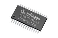 Infineon Technologies has announced that its OPTIGA TPM (Trusted Platform Module) will be the first device to comply with internationally recognised computer security requirements. The Common Criteria certification is an independent third party process said to help system and device manufacturers select trustworthy solutions.
This most recent version of the TPM standard is also claimed to addresses the security requirements of IoT devices. Trusted computing based on TPM root of trust hardware provides robust protection for such devices as gateways and routers used in smart homes, mobile devices as well as connected industrial and automotive systems.
Juergen Spaenkuch, head of platform security at Infineon, said: “Being the first supplier of a Common Criteria-certified TPM 2.0 device underlines our market and innovation leadership and opens the doors to new markets. Especially as the need for hardware-based security is expanding from traditional computing to include new IoT market segments.”
The OPTIGA product range is said to offer tailored security for the IoT, ranging from basic authentication products to advanced implementations for protecting integrity, authenticity and confidentiality of information.
Author
Tom Austin-Morgan
Source: www.newelectronics.co.uk
 A team of scientists and engineers from Harvard’s School of Engineering and Applied Sciences has demonstrated a rechargeable battery that, it claims, could make storage of electricity from intermittent energy sources safe and cost-effective for residential and commercial use.
The work builds on the earlier development of a flow battery, in which rechargeability is provided by chemical components dissolved in liquids contained within the system.
According to the researchers, the active components in most flow battery designs are metal ions dissolved in acid. However, the team said, these metals can be expensive, corrosive, tricky to handle and kinetically sluggish.
Previously Professor Michael Aziz and his team demonstrated a flow battery that replaced metals with quinones, organic molecules featuring in biological processes like photosynthesis and cellular respiration. While quinones formed the negative side of the battery, the positive side relied on a bromine bearing electrolyte. Looking to replace this, the team has used ferrocyanide ions.
“This is chemistry I’d be happy to put in my basement,” said Prof Aziz. “The non toxicity and cheap, abundant materials placed in water solution mean that it’s safe – it can’t catch on fire – and that’s huge when you’re storing large amounts of electrical energy anywhere near people.”
Ferrocyanide, which is soluble and stable in alkaline solutions, is paired with a quinone compound that is also soluble and stable under alkaline conditions. Because it is non-corrosive, the flow battery system components can be constructed of simpler, less expensive, materials such as plastics.
Author
Graham Pitcher and Tom Austin-Morgan
Source: www.newelectronics.co.uk