Electronics News
Archive : 25 October 2015 год
 Researchers from Brown University and Harvard University have developed a way to control light from phosphorescent emitters at very high speeds. The technique provides an approach to modulation that could be useful in silicon-based nanoscale devices, including computer chips and other optoelectronic components.
"Our results demonstrate relatively fast modulation from fundamentally slow phosphorescent light emitters," said Rashid Zia, associate professor of engineering and physics at Brown. "We think this could help make phosphors useful in a variety of new systems and settings."
Phosphors are extremely efficient because much of the energy they use is converted into light as opposed to heat. But they have a slow optical lifetime, meaning it takes a relatively long time for them to return to the ground state after being excited. As a result, phosphors can't be turned on and off very quickly.
That property is bad for optical modulation, a process that often involves flipping the light on and off to encode information. But in this latest work, Zia and his collaborators took a different approach to modulation.
Zia said: "Instead of changing how much light is coming out, which can only be done slowly in phosphor emitters, we came up with a system that changes another quality of that light, namely the colour or spectrum of light emission, by rapidly changing the environment around the emitter."
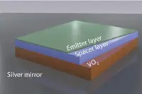
The work was led by Sebastien Cueff, a postdoctoral researcher in Zia's lab. Cueff started with an emitter made of erbium ions, a phosphor that is used in fibre-optic telecommunication networks. He combined that with a material called vanadium dioxide (VO2). VO2 is a phase-change material that, when pumped with energy, quickly changes from a transparent insulating state to a reflective metallic state. This change in reflectivity switches how nearby erbium ions emit light. As the VO2 changes phase, the erbium emissions go from being generated mostly by magnetic dipole transitions, to being generated mostly by electric dipole transitions. Those two emission pathways have distinct spectra, and the modulation back and forth between the two can be used as a means to encode information.
The researchers showed that this direct modulation of light emission could be done as quickly as the VO2 phase could be changed, which is much faster than the speed at which erbium can be turned on and off. The test system used in these initial experiments showed that the system could be switched three orders of magnitude faster than the optical lifetime of erbium.
This could enable the use of phosphors in new applications, such as optical communications networks on computer chips.
Prototype on-chip networks have used semiconductor lasers as light emitters. They can modulate very quickly, but they have downsides. Semiconductors can't be grown directly on a silicon chip, so fabrication can be difficult. Using indirect means of modulation - interferometers, for example - makes for bulky systems that take up a lot of real estate on a chip. What's more, semiconductor lasers are not particularly efficient: they produce a lot of heat along with light.
Erbium and other phosphors, on the other hand, can be deposited directly on silicon, making fabrication easier. There is still more work to be done to get such a system up to a speed that would be useful on a chip, but Zia and his colleagues believe it is possible.
Author
Tom Austin-Morgan
Source: www.newelectronics.co.uk
 Researchers from the Naval Research Laboratory (NRL) in Washington, DC have demonstrated that a combination of two technologies – one to create a thin film and the second to ‘cut’ designs from the film – could be a way to create custom electronic components.
The approach combines the attributes of laser induced forward transfer, or LIFT, with polymer assisted deposition (PAD). In LIFT, a laser beam vaporises a thin layer of solvent and ejects the ink or paste from the film. PAD works by dissolving metal salts in a solution containing polymers and spreading this in a thin layer, which is then heat cured to decompose the polymer.
The NRL team is working with inks containing vanadium dioxide (VO2), which undergoes a ‘sharp’ semiconductor to metal phase transition near room temperature. This, says the team, makes it suitable for applications such as chemical sensors, electrical and optical switches and coatings that change colour with temperature.
“There has not been much overlap between groups that study PAD and those that study LIFT,” said NRL fellow Eric Breckenfeld. “We are one of the first groups to try combining the two techniques.”
Breckenfeld and his colleagues explored a variety of solvents and heating steps to optimise the growth of VO2 films on glass and crystalline substrates, then experimented using LIFT to print patterns with the PAD solutions.
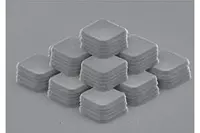
So far, the team has successfully printed simple patterns. Breckenfeld said the results show that LIFT and PAD technologies combined could directly print a range of commercially attractive electronic materials.
Pic: Eric Breckenfeld/NRL
Author
Graham Pitcher
Source: www.newelectronics.co.uk

